CNT Pellicles Explained: Hydrogen, Lifetime, and the Demand Math
Part 2: A technical follow-up on my Canatu piece, EUV pellicle chemistry, ASML’s guidance on CNT lifetime, and why Samsung’s Taylor fab matters.

Because my recent, very detailed article on Canatu received an unexpectedly positive response, I decided to write a shorter follow-up piece. Its purpose is to address several questions and points of confusion whose answers are not always intuitive, or are only sparsely available in public sources.
In this follow-up, I will focus primarily on CNT pellicles. In my original article, I covered Canatu’s potential customers in depth, explained its unique dry deposition manufacturing method, and attempted to build a model estimating future CNT pellicle demand under the assumption that this material could become the new industry standard in advanced chip manufacturing.
PART I: The Missing Link in the AI Supply Chain: Why I’m Betting on Canatu
The main topics of this supplementary article will therefore be hydrogen chemistry in EUV environments, how to properly think about wafers, exposures, and EUV layers when estimating pellicle demand, and my recent findings on what ASML has publicly stated regarding current CNT pellicle lifetime and adoption. I will also add a short note on DRAM and the Taylor fab example, as these may matter for the total addressable market and were intentionally not included in my original pellicle demand model.
CNT Pellicles & Hydrogen
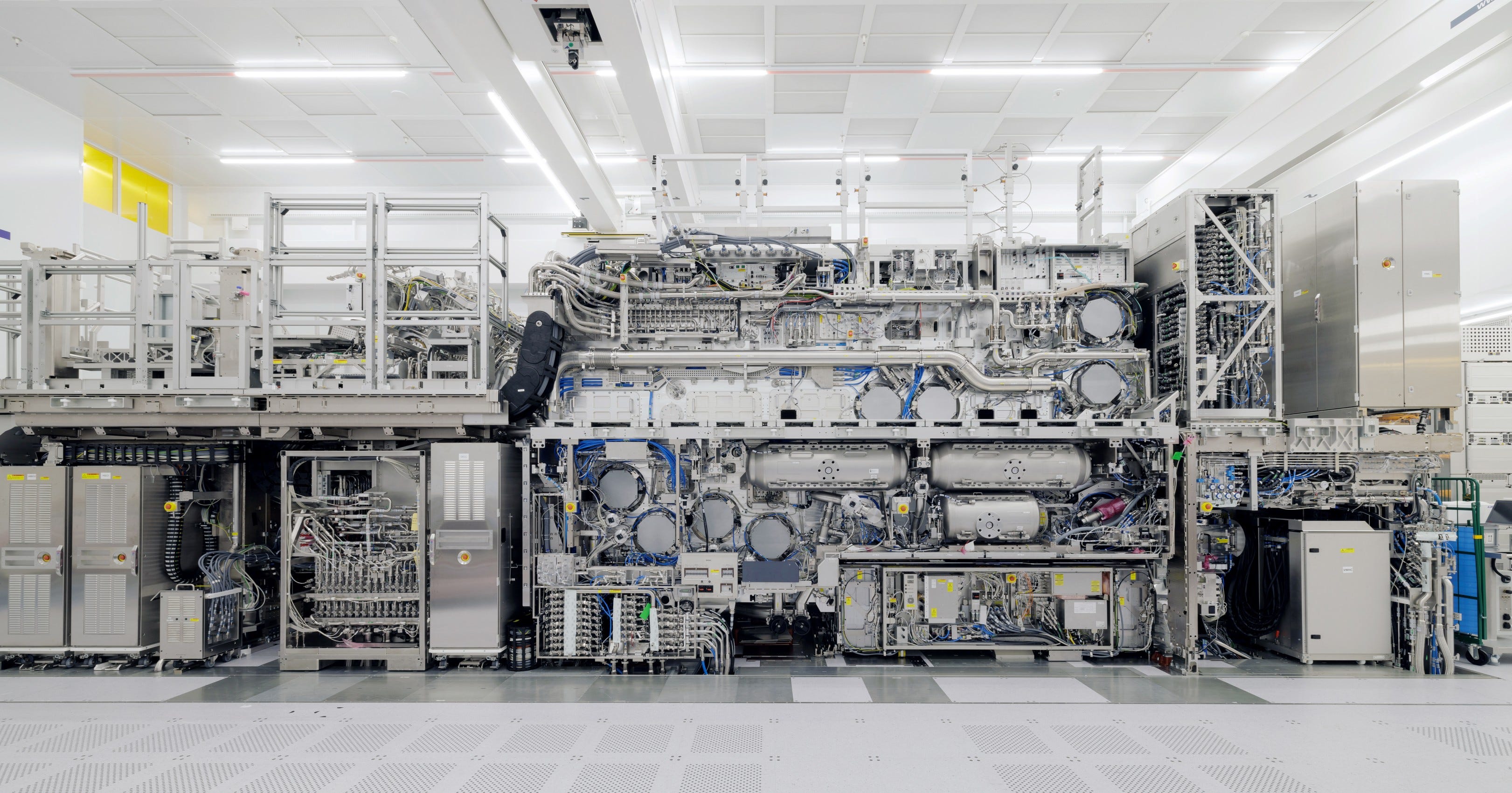
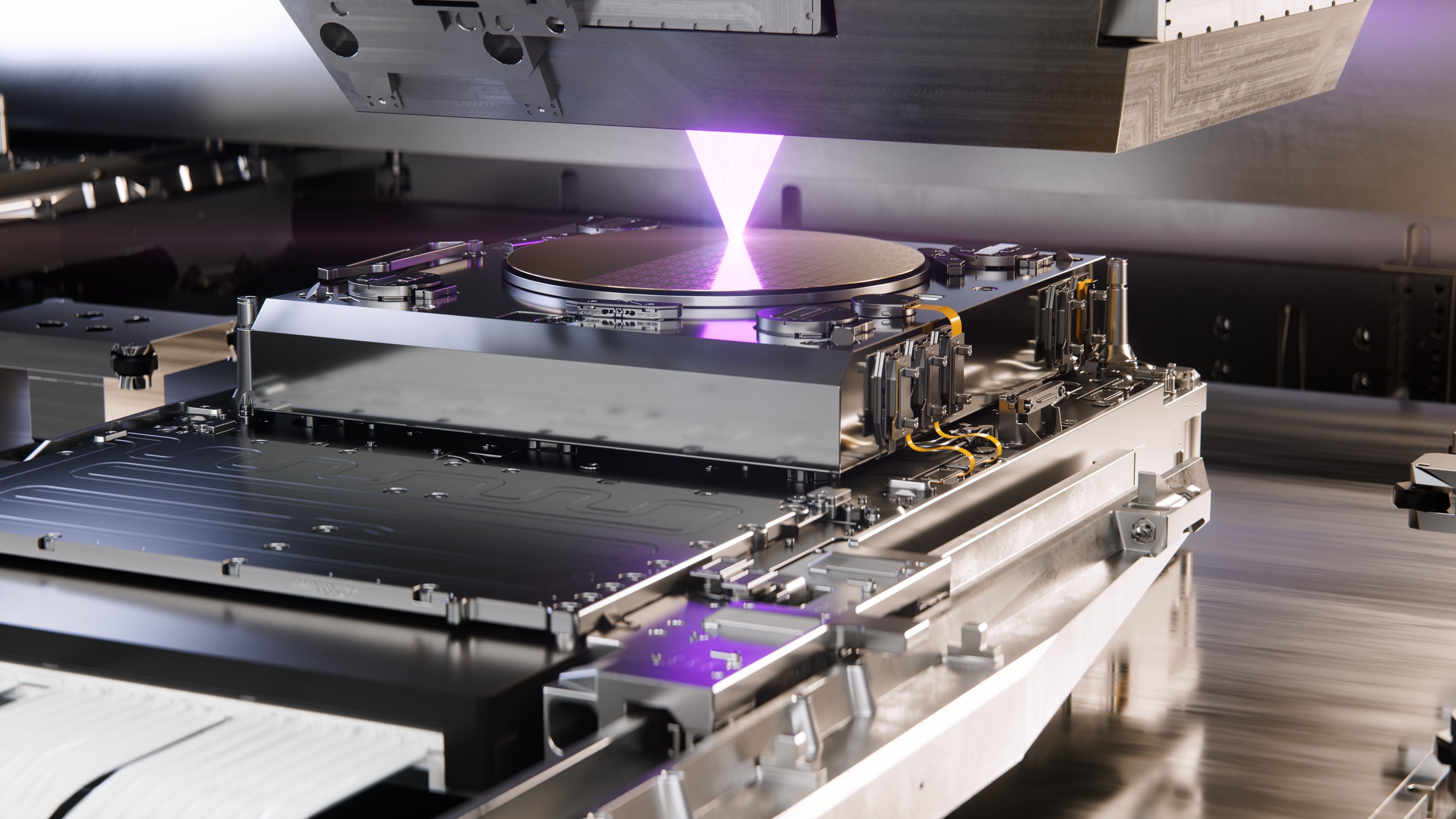
What do you do on weekend evenings? I decided to spend mine digging a bit deeper into EUV lithography. I picked up a few chapters of Extreme Ultraviolet Lithography by Harry J. Levinson, focusing mainly on masks and pellicles. One thing immediately stood out to me, and it’s something I had not fully appreciated before.
CNT pellicles are made of carbon, while EUV scanners operate in a hydrogen-rich environment. Hydrogen is intentionally present inside EUV tools to suppress carbon contamination on mirrors and masks. However, under intense EUV radiation, hydrogen becomes chemically active. In this environment, EUV photons can accelerate reactions between hydrogen and carbon, gradually converting carbon into volatile hydrocarbons such as methane.
This interaction turns out to be a key technical challenge for CNT pellicles.
Over time, this hydrogen-driven erosion can slowly degrade carbon nanotube structures, directly impacting pellicle lifetime. This is why protective coatings are often considered necessary. However, coatings introduce a delicate trade-off: while they can improve chemical resistance and durability, they also add optical thickness and increase light scattering, both of which are undesirable in EUV lithography.
In solution-based or polymer-assisted CNT pellicle approaches, commonly associated with suppliers such as Mitsui or Lintec, nanotubes are typically processed using liquids, binders, or transfer layers. These additional materials can help stabilize the structure and protect against hydrogen, but they inevitably leave residual chemistry in the membrane. As a result, achieving long lifetime often comes at the cost of reduced optical performance or increased scattering.
By contrast, dry-deposited CNT pellicles, as pursued by Canatu, are formed directly from the gas phase without any liquid processing or polymer binders. This results in exceptionally clean nanotube networks with minimal residual contamination. Because the underlying structure is purer and more uniform, hydrogen resistance can be addressed with much thinner and more controlled protective layers, or in some cases by material optimization alone.
This technological cleanliness is not just an academic detail. It directly affects how effectively lifetime can be improved without sacrificing EUV transmission. In a regime where CNT pellicles already outperform alternatives in transparency, the industry challenge is no longer whether CNT works, but how far lifetime can be extended. And this is precisely where dry deposition offers a structurally stronger optimization path.
A Simple Way to Think About Pellicle Demand
On the forum where we actively discuss Canatu, I shared a very simplified way of thinking about pellicle demand. It’s not meant to be precise or fab-accurate, but rather a conceptual tool to understand the main drivers behind pellicle consumption.
How I try to estimate:
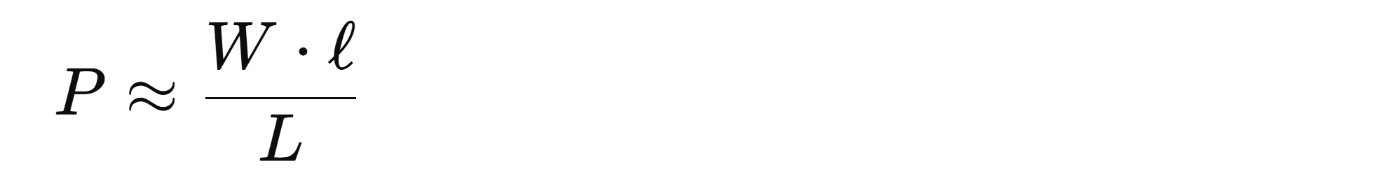
Where
P = pellicles / year (per tool)
W = wafers / year (per tool)
ℓ = EUV layers per wafer ≈ EUV exposures per wafer
L = pellicle lifetime (in exposures)
This equation also implicitly assumes that all EUV layers use CNT pellicles, which is likely not (yet) true today. One could add an adoption-rate factor to account for partial usage, but for the sake of clarity, I’ll keep things simple here.
Looking at the equation, the first part; wafers per year, is relatively easy to estimate. ASML has consistently increased wafer throughput per EUV scanner over time.
Just to put things into perspective: between 2018 and 2022, wafer output per tool roughly doubled from about 1,500 wafers per day to around 3,000. Today, estimates are closer to 4,000 wafers per day per ASML machine.
Considering the complexity of EUV lithography, that pace of improvement is remarkable. It’s not hard to see why EUV scanners are often described as the most complex machines ever built by mankind.
The second component; EUV exposures per wafer, can also be approximated reasonably well. In simplified terms, we can think of this as the number of EUV layers per wafer. If a wafer has, say, 14 EUV layers, it will require roughly 14 EUV exposures. This approximation is not perfect, but it is directionally correct and sufficient for a first-order model. The real problem starts with the third variable: pellicle lifetime.
Pellicle Lifetime
At the moment, pellicle lifetime is extremely difficult to pin down. Some sources, often based on offline or accelerated testing, mention lifetimes of up to 20,000 exposure cycles. However, I came across an ASML-related academic paper from late 2025 that suggests current CNT pellicle lifetime is closer to 5,000 wafer exposures.
Interestingly, the same paper explicitly states that:
“EUV pellicle innovations are speeding up with the introduction of Carbon Nanotube (CNT) pellicles. CNT pellicles outperform metal silicide capabilities on transmission.”
It also makes clear that:
“We have seen data coming from various customers and they all report to us well, that the imaging is OK. So that's not the issue. So the focus should really be on extending lifetime. We do our part in the scanner, we try to reduce the hydrogen pressure as much as possible. Of course that has its limits.”
In other words, CNT pellicles have already won on optical performance, especially transmission, but lifetime is now the dominant bottleneck. This is not a static parameter; it is something that is actively being optimized and will likely evolve over the coming years.
That uncertainty is precisely why, in my original demand model, I did not rely on a single lifetime assumption. Instead, I used three different scenarios, each based on a different pellicle lifetime, to capture a realistic range of possible outcomes rather than pretending we know the exact number today.
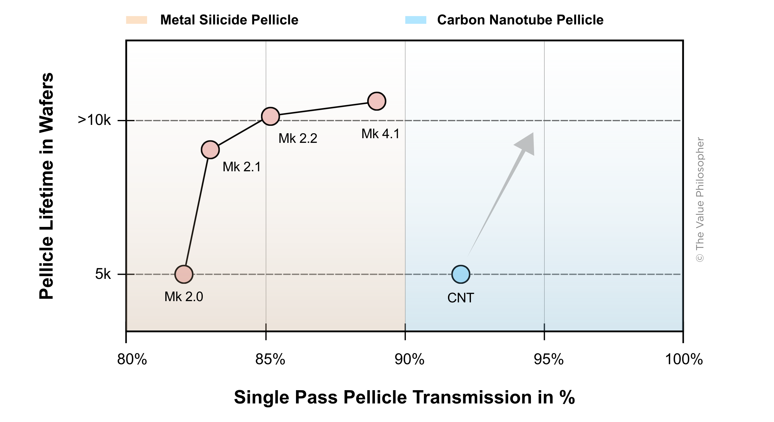
As I studied the paper, I took the original data and recreated the chart to better understand what it was actually showing. The Mk labels refer to successive generations (Mark revisions) of metal-silicide EUV pellicles, each representing incremental improvements in transmission, thermal handling, and durability over time. What stands out immediately is that CNT pellicles do not appear as just another Mk step, but as a new starting point on a different performance curve.
Even at this early stage, CNT pellicles already exceed the transmission levels reached only after multiple generations of metal-silicide development. As a result, the industry focus has clearly shifted away from optical performance and toward extending CNT pellicle lifetime.
The good news is that CNT pellicles are not a speculative side project. ASML clearly expects them to play a role going forward. As stated directly in their materials:
“ASML will be ready to support carbon nanotube pellicles to further mitigate mask defectivity. Pellicle film development is done by third parties; ASML facilitates the certification process for scanner usage.”
This confirms that CNT pellicles are already embedded in ASML’s forward-looking ecosystem. The open question is no longer if CNT pellicles will be used, but how fast lifetime improvements can be achieved, and how that translates into real-world pellicle demand.
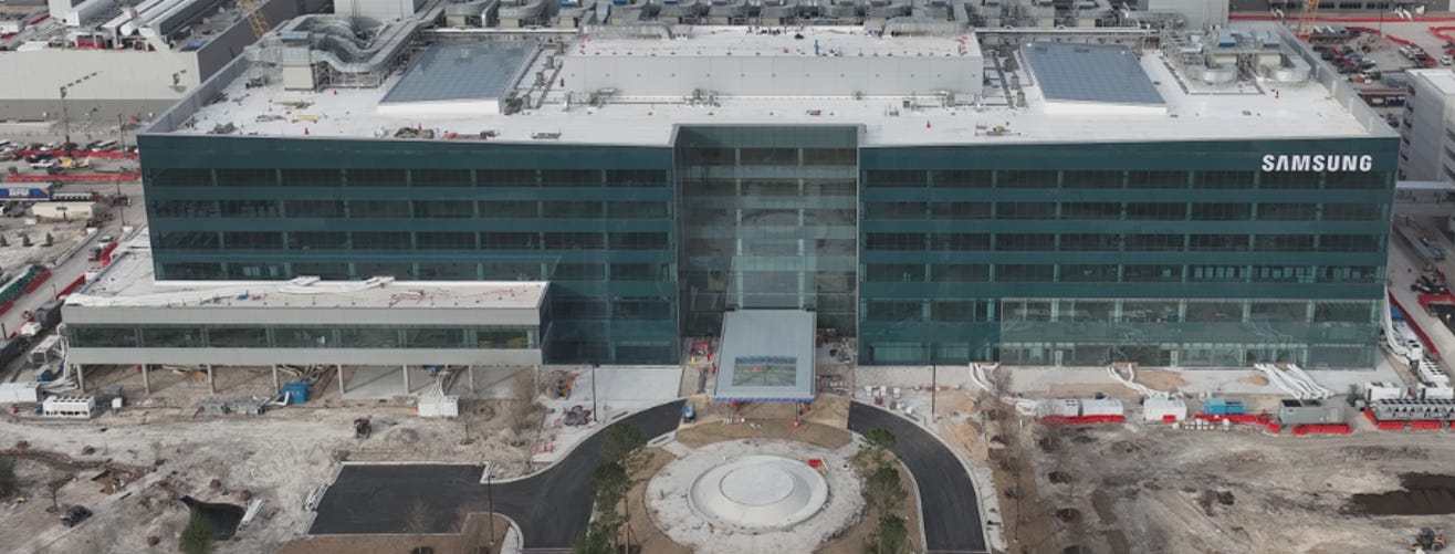
Samsung Taylor Fab News
Last week, Samsung delivered an important signal that materially changes the near-term outlook for EUV pellicles.
According to multiple Korean media outlets, Samsung is accelerating the ramp-up of its Taylor, Texas fab. Trial runs of EUV lithography tools are expected to begin as early as March, with full-scale production targeted for the second half of 2026. Even more importantly, Samsung is reportedly upgrading the originally planned 4nm node to 2nm, placing Taylor firmly in the leading-edge category.
What makes this development particularly relevant in the context of CNT pellicles is a related infrastructure order. ETNews reports that Samsung has awarded a KRW 25 billion (around $18 million) contract to South Korean supplier FST for EUV pellicle handling equipment at the Taylor site. This equipment supports both conventional metal silicide pellicles and next-generation carbon nanotube (CNT) pellicles.
This is not a marginal investment. You do not deploy tens of millions of dollars into pellicle handling infrastructure unless you expect pellicles to be consumed at industrial scale.
A Simple Estimate
Following the announcement, I was asked on X how I arrived at an estimate of roughly 2,000 pellicles per year for the Taylor fab. The calculation is intentionally simplified, but the logic is transparent.
Logic Only
Samsung has indicated that Taylor is designed as a high-volume, leading-edge logic fab. Using conservative assumptions:
Target volume: ~50,000 wafers per month
→ ~600,000 wafers per yearEUV intensity: ~25 EUV layers per wafer (typical for a 2nm-class logic node)
Total EUV exposures:
→600,000 × 25 = 15 million exposures per year
As mentioned earlier, pellicle lifetime is the largest uncertainty. Public data is scarce, especially for high-power, High-NA–class conditions. Based on available ASML presentations and academic literature, a working estimate of ~7,500 exposures per pellicle under these conditions is reasonable, though it could ultimately prove higher or lower.
15,000,000 ÷ 7,500 ≈ 2,000 pellicles per year
Whether the real number turns out to be 1,500 or 3,000 is not the key takeaway. The important point is that baseline 2nm logic production alone is sufficient to saturate the annual output of a single CNT pellicle reactor.
What About DRAM?
The estimate above intentionally considers logic manufacturing only.
DRAM production follows a structurally different pattern. While DRAM wafers typically require significantly fewer EUV layers per wafer, roughly in the range of 5 to 8, the total wafer volumes are substantially higher. As a result, even with lower per-wafer EUV intensity, cumulative exposure counts can become comparable to logic manufacturing when operated at scale.
Using a rough illustrative example:
DRAM volume: ~200,000 wafers per month
EUV layers: ~6 per wafer
That yields:
200,000 × 12 × 6 ≈ 14.4 million EUV exposures per year
At similar lifetime assumptions, DRAM alone could imply another 2,000 pellicles per year. In other words, when both logic and memory are considered, total pellicle demand at Taylor could plausibly approach around 4,000 units annually.
Why This Matters
The strategic implication here is not the exact pellicle count, but the capacity mismatch it reveals. FST is currently believed to operate a single Canatu-licensed CNT reactor. Even under conservative assumptions, demand implied by Taylor-level production would push such a setup to full utilization very quickly.
From a supply-chain perspective, this strongly points toward the need for additional reactor capacity, N+1 redundancy, and a broader multi-year capex expansion cycle tied to High-NA adoption and advanced-node scaling. For Canatu, each incremental reactor is therefore not merely a one-off hardware sale, but a gateway to long-duration, high-margin licensing and consumables revenue that can compound over time.
Talk soon!
25.1.2026 ~ The Value Philosopher
If you enjoyed this article and want to read more about the intersection of macroeconomics, technology, and investing, consider subscribing.
Disclaimer: I cannot guarantee the accuracy or timeliness of the information provided herein. This article does not constitute financial advice, an investment recommendation, or a factual basis for your investment decisions. Please conduct your own due diligence.
Great work, thanks for sharing your knowledge