The Missing Link in the AI Supply Chain: Why I’m Betting on Canatu
Finding the hidden infrastructure essential for the next generation of chips. Hyperscalers are expensive. I found the pick and shovel play hiding inside the world’s most advanced lithography machines.

How Expensive Silver Led Me to Carbon Nanotubes
One weekend afternoon over coffee, I was watching precious metals charts and thinking about the incredible momentum silver saw in late 2025. The price was attacking the $70 per ounce mark back then (it is $90 as of early 2026).
I just sat there wondering what this move, which effectively rewrote the history books and looked like a roller coaster ride to many investors, actually meant fundamentally.
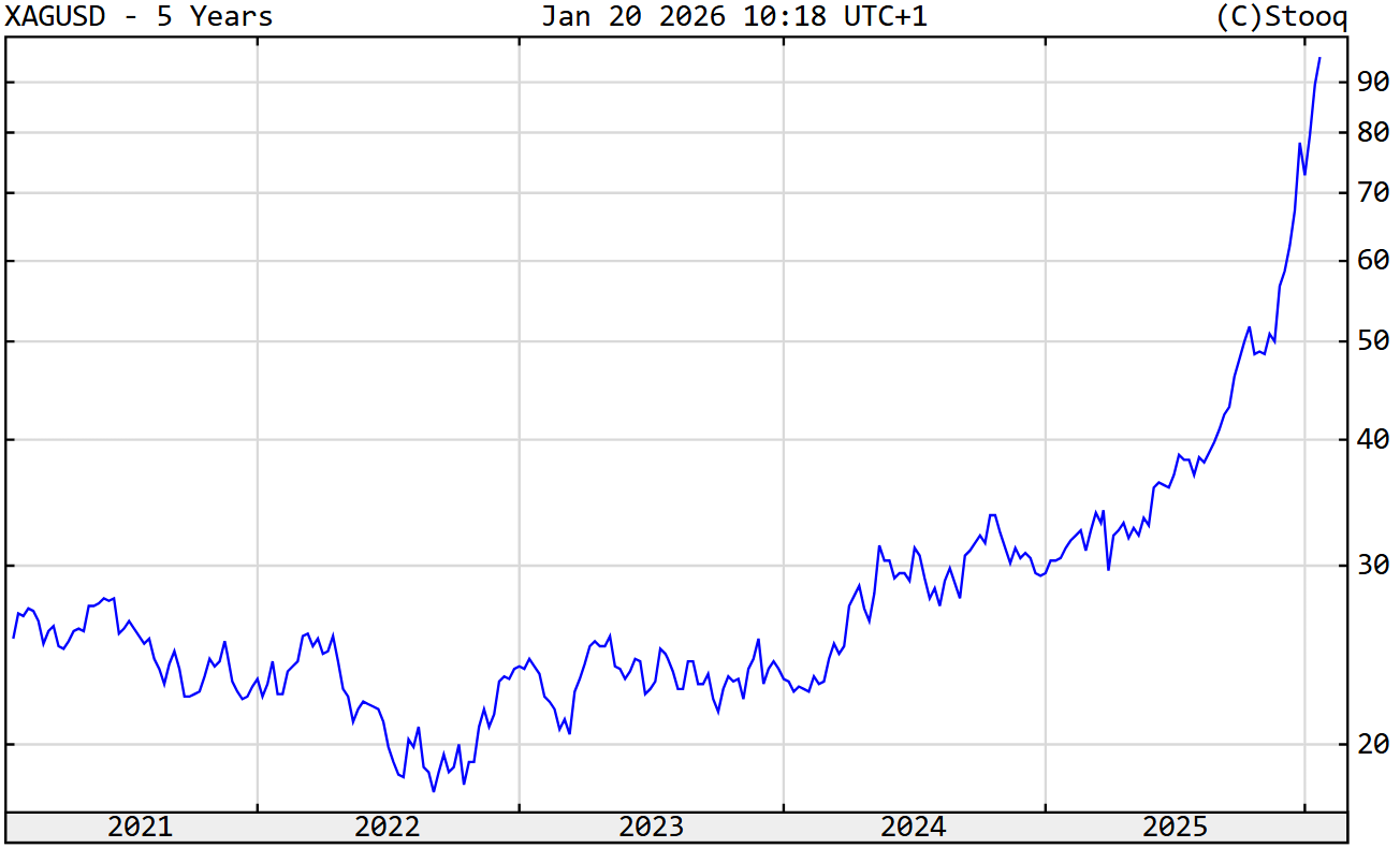
It wasn’t a random or isolated blip, but the culmination of a perfect storm. From a macro perspective, this sharp move is the logical conclusion of a long-forming situation where several major structural factors intersected over a few years. One was the chronic deficit in the silver market. 2025 marked the fifth consecutive year where global silver consumption outstripped mining supply. The gap had long been plugged by stockpiles in London and COMEX warehouses, but these gradually hit critically low levels, effectively scraping the bottom of the barrel.
Another key factor is the transformation of the solar industry. The mass transition to more efficient TOPCon photovoltaic cells brought technological progress, but significantly increased material intensity. These new cells consume approximately 20–50% more silver than older technologies, resulting in the solar sector absorbing a substantial portion of available global production.
Pressure on the silver market was further intensified by the rapid boom in artificial intelligence and the associated build-out of massive data centers. These are extremely raw-material intensive, particularly regarding copper for cabling and cooling, and silver used in connectors, semiconductors, and electronic components. Given that copper and silver function as closely linked industrial twins in practice, a shortage in one metal automatically began pushing up the price of the other.
The result of this accumulation of factors was market panic. Industrial buyers, terrified by the real threat of supply chain interruptions, began buying regardless of price to build above-average inventories. This stockpiling process triggered a classic squeeze, subsequently shooting the price of silver to extreme highs.
When the Train Has Left the Station
Looking at the almost vertical price chart, I had to admit an uncomfortable truth, I had missed this phase of market mania. Boarding a moving train at around $70, whether through physical metal, miners, or recyclers, would have meant taking on disproportionate risk at that moment. The era of easy money was clearly in the past, and the market was showing clear signs of overheating. Attempting to ride this wave would have been closer to gambling than rational investing.
Instead of succumbing to FOMO, I started thinking one step ahead. I describe my approach to finding opportunities in my recent article, specifically in the Market Wave Dynamics section. I asked myself a question: What comes next?
Mineral reserves are finite. If silver and copper prices rise to levels that start threatening manufacturers’ margins, the market will desperately seek a way out. The economic pressure to replace these precious metals has never been higher.
I gradually came to the conclusion that the real potential no longer lies in the metal itself, but in its substitution. The key question became whether it is possible to replace these materials in certain manufacturing segments. Is there a specific chemical compound, advanced composite, or nanotechnological material that could at least emulate, or perhaps even surpass, the properties of silver?
It’s Not Just Price, It’s Physics
I’m not a chemical engineer or a material physicist; my competitive edge doesn’t lie in the lab, but in identifying structural market trends. Yet, it was clear that traditional conductors, such as silver, copper, or the ubiquitous indium tin oxide (ITO) used in displays, are hitting fundamental physical walls. They are fragile.
In an era racing toward flexible displays, heated curved glass for autonomous vehicles, and wearable electronics, this is a critical bottleneck. When an ITO or silver layer bends, it cracks. The industry, therefore, isn’t just hunting for cheaper silver. It’s searching for a material that is conductive, transparent, and above all, mechanically incredibly durable and flexible.
I went looking for someone capable of solving this problem through advanced chemistry and nanotechnology. That search led me to a Finnish trail, and a company called Canatu.
Disclaimer: I cannot guarantee the accuracy or timeliness of the information provided herein. This article does not constitute financial advice, an investment recommendation, or a factual basis for your investment decisions. Please conduct your own due diligence.
Canatu
My hunt for a technological substitute for silver eventually led my research to Finland, specifically, to the city of Vantaa. This is where Canatu is headquartered.
At first glance, it didn’t look like the next big thing. It is a relatively small company with a market capitalization of around €300 million. But what stopped me in my tracks was the founding year: 2004.
Immediately, a red flag popped up in my mind: If they’ve been around for over 20 years, why hasn’t anyone heard of them? Why aren’t they a giant by now?
This fact naturally raises a legitimate question. The answer turns out to be intrinsically linked to the very nature of their business. Canatu is a textbook example of a deep-tech company. This isn’t a software project with a short innovation cycle; it is a technology spin-off from the prestigious Aalto University that has spent a substantial part of its existence in a laboratory environment, developing a new form of carbon nanomaterials and systematically building an extensive patent portfolio.

Such development is characterized by an extremely long incubation phase, high capital intensity, and technological uncertainty. That is precisely why Canatu is only now reaching the stage that is critical for investors: the inflection point where research and development gradually transform into industrially scalable production and commercial applications.
When I started digging into what their technology can actually do, I realized I hadn’t just stumbled upon an interesting stock, I had fallen down a technological rabbit hole.
Carbon NanoBuds (CNB™)
To truly grasp Canatu’s investment potential, we must look under the hood at the technological core of its business. The keystone of their entire strategy is a proprietary nanomaterial known as Carbon NanoBuds (CNB™), which represents a fundamental qualitative shift from previously known carbon nanostructures.
Carbon nanotubes (CNTs) have been known to the scientific community for decades, prized for their extraordinary mechanical strength, high electrical conductivity, and low weight. Yet, despite these theoretically exceptional properties, their practical industrial application has long hit significant walls. Standalone nanotubes tend to slide against one another, creating weak contacts and exhibiting unstable electrical and mechanical properties in macroscopic layers. These characteristics significantly complicate their integration into reliable, industrially manufactured conductive structures.
Canatu’s research team solved this problem by developing a unique hybrid nanostructure that combines classic carbon nanotubes with spherical fullerene-like molecules. The result is a material where nanoscopic structural buds are anchored to the surface of the nanotubes. These protrusions fundamentally alter how individual nanostructures interact.
Instead of sliding freely, the elements mechanically and electrically interlock, creating a stable, highly interconnected three-dimensional conductive network.
This architecture decisively overcomes the limitations of traditional conductive materials used in electronics, such as silver and indium tin oxide (ITO). While metal or oxide layers achieve good conductivity at the cost of mechanical brittleness, CNB™ based layers retain full electrical functionality even under extreme mechanical deformation.
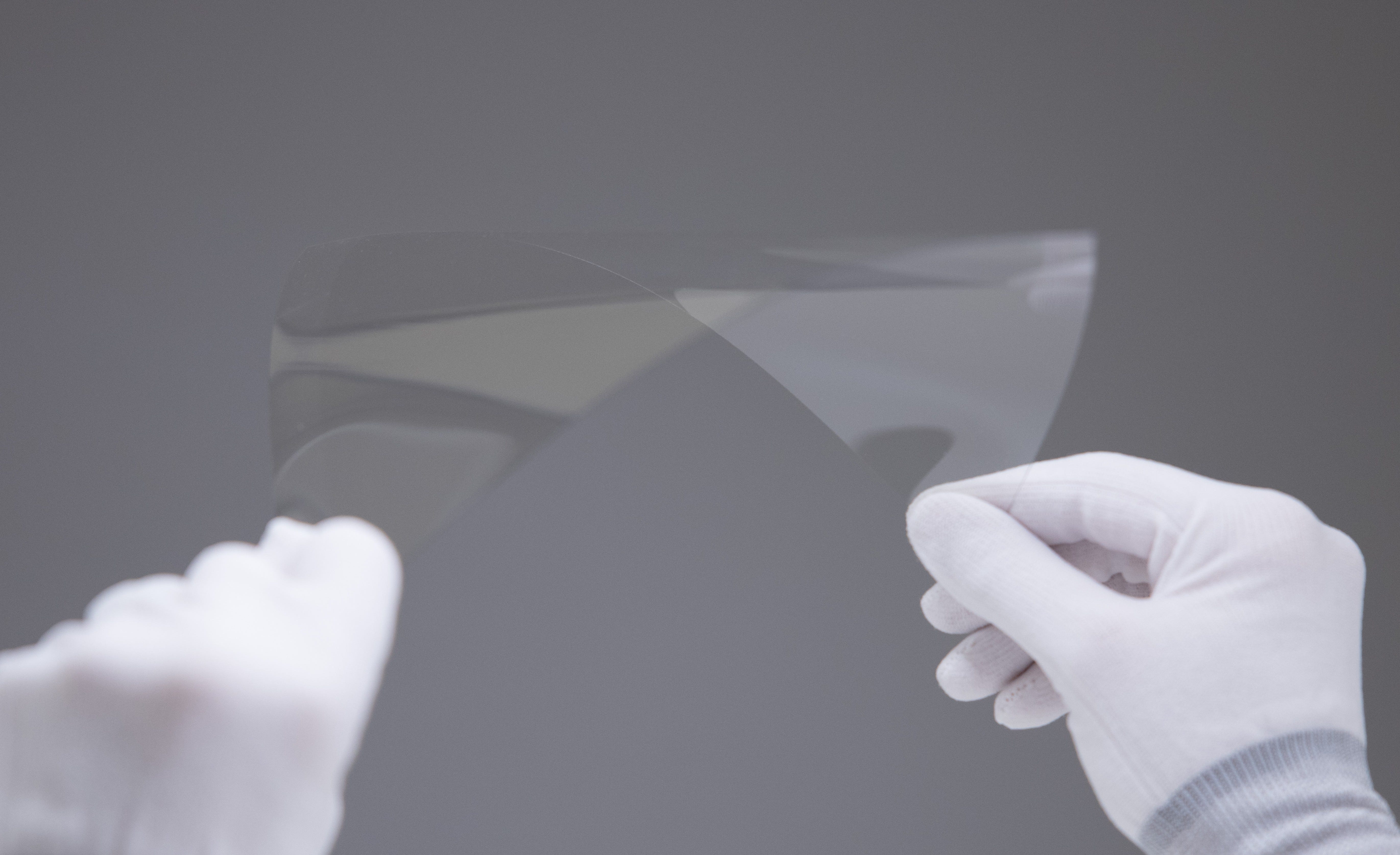
The material is optically transparent and capable of elastic elongation up to approximately 200% of its original length without breaking conductivity.
From an industrial application standpoint, this is a major technological breakthrough. Modern electronic design is increasingly trending toward flexible, curved, and spatially shaped solutions, from displays and sensor layers to heated glass, wearable electronics, and integrated textiles. Traditional conductive materials fail in these segments precisely because of their brittleness. CNB, by contrast, enables the creation of conductive layers that maintain functionality even under repeated bending, tension, and complex 3D shaping.
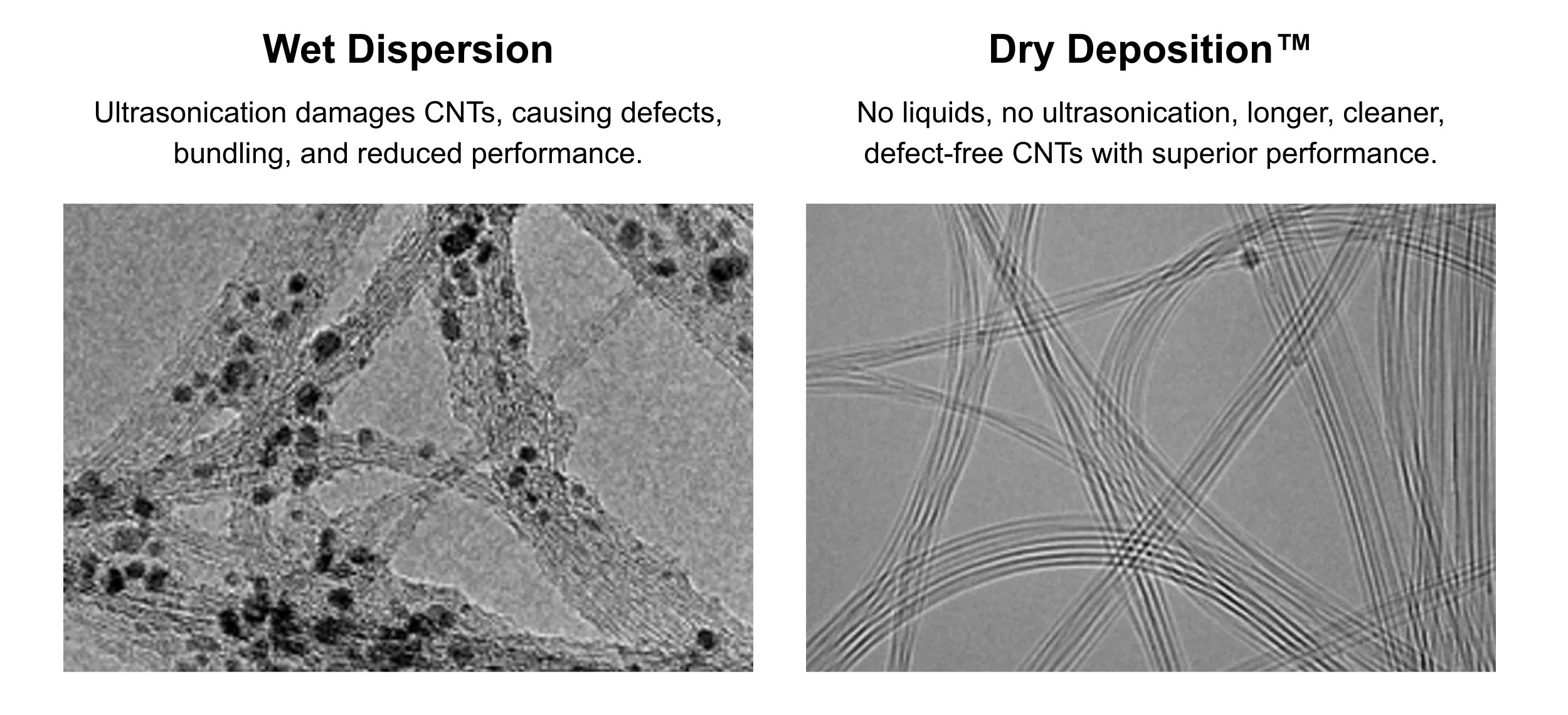
However, the existence of an advanced material alone does not constitute a commercial advantage. The deciding factor is the ability to produce this material reproducibly, at high quality, and under economically sustainable conditions. This is where traditional competition often hits limits associated with so-called wet processing methods, which require toxic solvents, multi-step cleaning, and costly quality control.
Here, Canatu holds another crucial technological lead in the form of its proprietary manufacturing method. This allows for the production of CNB™ without liquid processes, creating a direct bridge between laboratory innovation and industrial scalability. The following part will be a bit technical, but it’s worth it, I promise.
Dry Deposition™
To achieve material properties that physics previously deemed impossible, Canatu had to eliminate the greatest weakness of traditional nanotechnologies: liquids.
Conventional carbon nanotubes, like those known from EV batteries, are produced as a black powder that is subsequently mixed into liquid slurries and applied like ink. However, this process is often unusable for high-end tech applications. It is too dirty. It leaves behind chemical residues, solvents, and structural defects that degrade both conductivity and transparency.
Canatu’s answer is its proprietary method: Dry Deposition™
This manufacturing process defies the classic image of factory production and resembles a controlled physics experiment instead. At its heart is a vertical reactor. Carbon-containing gases and a catalyst are injected into the top. Inside the reactor, directly in the gas phase, carbon atoms spontaneously assemble into carbon nanotubes.
These nanotubes do not form on any solid surface, they are born in mid-air and are carried downward by the gas flow.
You can visualize it like snowflakes forming in clouds and slowly drifting to earth.
This eliminates complex chemistry, radically reducing operating costs and making the entire process not only greener but, crucially, scalable for mass production. It is this combination of a unique material and efficient manufacturing that creates the technological moat.
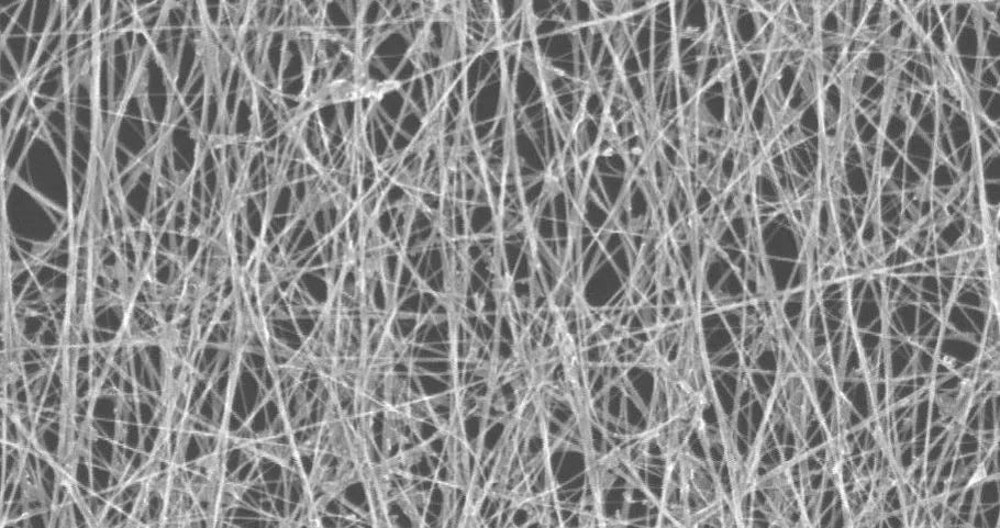
The Power of Randomness
At the bottom of the reactor lies a filter or substrate where these nanostructures land. The key is that they land completely at random. No regular grid or ordered pattern is formed; instead, a chaotic, entangled network of nanotubes is created.
This randomness, technically called a stochastic structure, is paradoxically the material’s greatest strength. If the nanotubes were oriented primarily in one direction, the material would have weak points and tear easily, much like wood splitting along the grain. A randomly entangled network, on the other hand, is mechanically stable in all directions, similar to felt or a very fine spiderweb.
Almost Nothing, Yet Everything
The resulting material is fascinating:
97% of its volume is empty space (air), and only 3% is actual carbon.
This gives the network a unique dual property: it is dense enough to physically trap even the smallest dust particles, yet empty enough for light and energy to pass through with almost zero loss. Canatu can transfer this network onto any surface without the use of adhesives, creating the cleanest, thinnest, and strongest transparent conductor in the world.
Whether it’s heating a car windshield or protecting the world’s most expensive microchips, the underlying principle remains the same.
"We could have an extremely dominant market position in the future in CNT pellicles. Currently, all presentations are based on CNT, we don't have information that any new technology or material is coming that could challenge this." - CEO Juha Kokkonen
So, what are the real-world applications of this material? The theoretical potential for this new technology is vast. However, in this article, I want to focus primarily on two current segments where the company sees its future: Automotive and Semiconductor.
1. Automotive
If we look at Canatu’s technology from a distance, we realize it’s not just a single product, but a universal technology platform. The very same material that solves problems in the lab also solves fundamental physical limits on the road: combining conductivity, transparency, and extreme flexibility.
Nowhere is this need more acute than in the dawning era of autonomous driving.
ADAS: The End of Frozen Sensors
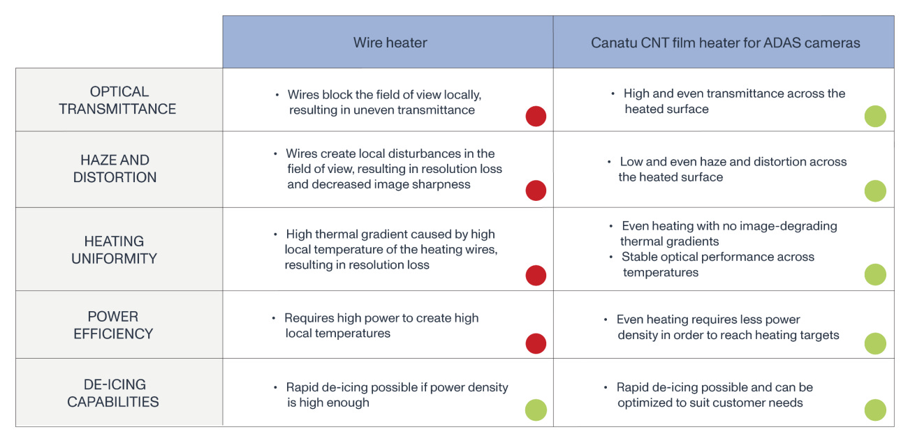
Modern vehicles are equipped with a growing array of sensors, cameras, radars, and LiDAR systems, which form the backbone of Advanced Driver Assistance Systems (ADAS). Yet, these sensors share a common weakness: their functionality is heavily impacted by weather conditions. Icing, condensation, or snow buildup can degrade input data quality in moments, leading to the limitation or complete deactivation of safety features.
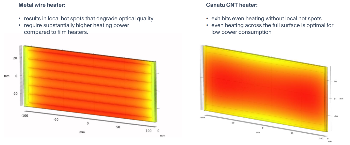
Traditional approaches to sensor heating and defogging are fundamentally incompatible with modern optical systems. Tungsten heating wires, commonly used in rear window defrosters, are unsuitable for cameras and optical sensors because they physically obstruct the field of view.
Indium tin oxide, while widely used as a transparent conductive coating, suffers from intrinsic brittleness. When applied to curved or complex geometries, such as the convex lenses of headlights or LiDAR units, it is prone to mechanical cracking, leading to rapid loss of electrical and functional reliability.
Canatu’s nanocarbon films overcome these limits. They are optically transparent, contain no visible structures (wire-free), and retain electrical functionality even when applied to complex 3D surfaces. Given that a modern car carries 5 to 10 of such sensors, we are talking about a market in the order of billions of units annually.
Tesla: Software vs. Physics
A logical objection might cross your mind: What about Tesla? They don’t use anything like this.
You are right. Elon Musk is famous for his drive to simplify manufacturing (the best part is no part) and cut costs. Tesla currently bets on solving icing with brute force, blowing hot air and letting software compensate for image imperfections.
However, if we are talking about true autonomous driving (Level 4 and 5), where the driver doesn’t need to pay attention, regulators in the EU and USA will be uncompromising. A camera cannot be blind for even a second. Physically removing ice with air takes too long and is energy-intensive. It is highly probable that legislation will eventually force even players like Tesla to switch to a dedicated hardware solution. At that moment, Canatu becomes the logical choice even for the skeptics.
Winter Range: The Battle for Every Kilowatt-Hour
Another significant application area is increasing EV energy efficiency in cold climates. Traditional cabin heating and window defogging systems rely on heating air via HVAC units. From a heat transfer physics perspective, this is inefficient; air is a poor conductor, and heating large glass surfaces requires significant energy.
Heating in extreme winter can reduce an EV’s range by a drastic 45%.
Canatu offers an elegant solution: transparent heating of the entire windshield surface. Instead of heating the air, energy is sent directly into the glass, which is much faster and orders of magnitude more efficient. This addresses energy consumption and allows for more efficient use of the traction battery capacity, especially in winter conditions when EV range is under the most stress.
DENSO Partnership
Proof that this isn’t merely a laboratory concept comes in the form of a strategic partnership with the Japanese giant, DENSO.
For context, DENSO is a tier 1 supplier delivering components to the world’s leading automakers: Toyota, Honda, Volkswagen, BMW, and Mercedes-Benz. The collaboration, announced in early January, 2026, focuses specifically on integrating Canatu’s technology into windshields and headlights.
The fact that such an industrial colossus is investing capacity into the implementation of nanocarbon films is, for me as an investor, the strongest signal of de-risking. The technology is mature enough for mass production.
Long-term Potential: Solar Roofs
Beyond the main applications, long-term development projects are worth noting, particularly in the realm of integrated solar roofs.
Current automotive solar panels achieve an efficiency of approximately 25%, which limits their practical benefit. Canatu is working on tandem solar cell technology, where a nanocarbon layer could help boost efficiency into the 35–40% range. At that level, it would become a meaningful source of additional energy, capable of generating tangible daily range for the vehicle.
While the automotive sector represents a visible and easily understood application of Canatu’s technology, a surprise awaited me during a deep dive into their financial statements and projections.
To my astonishment, the company’s management expects that the largest and most profitable revenue streams in the future will not flow from cars, but from chip manufacturing.
2. Semiconductors
Here we enter a sector where purity translates to billions and where Canatu plays a low-profile but strategically critical role. This section will be even more technical, I apologize, but it is vital to the thesis.
It is in the semiconductor industry that Canatu’s technology enters an environment where even a seemingly marginal material improvement can have multi-billion dollar economic impacts.
EUV Lithography: The Game of Nanometers
The production of the most advanced semiconductors today is practically unthinkable without extreme ultraviolet lithography (EUV). It is the only commercially viable method that enables chip production at the level of just a few nanometers, powering the key processors for artificial intelligence, data centers, and high-end consumer electronics. These chips are found, for instance, in accelerators from NVIDIA and AMD, or in the latest generations of processors for Apple devices.
The entire EUV process takes place in an extremely controlled environment, one of the cleanest manufacturing spaces on Earth. The fundamental element of this process is the photomask (or reticle), a high-precision template carrying the blueprint of the future chip. The price of a single photomask commonly runs into the hundreds of thousands of dollars, and any damage or contamination has immediate and severe financial consequences.
The Critical Role of the Pellicle
To protect the photomask from contamination, an ultra-thin protective membrane known as a pellicle is used. Its job is to prevent even the tiniest dust particles from landing on the mask, while simultaneously allowing EUV radiation to pass through.
This requirement is extraordinarily demanding because EUV radiation has very high energy and interacts with materials in a fundamentally different way than visible light.
When Physics Hits a Wall
Current industrial solutions based on silicon or metal membranes are reaching their physical limits. These materials are again, mechanically brittle. As the power of lithography sources increases, they suffer from overheating, deformation, and in extreme cases, destruction.
Yet, increasing the power of EUV sources is absolutely essential to ensure higher manufacturing throughput and the economic efficiency of chip production.
Chip manufacturers like TSMC, Samsung, and Intel are thus under immense technological pressure. They need a material that is simultaneously mechanically stable, thermally resistant, and as transparent as possible to EUV radiation.
The Limits of Silicon Membranes
The current industry standard relies on membranes based on polycrystalline silicon and metal silicides. These materials can be characterized as extremely thin but mechanically brittle layers, whose properties cannot be significantly improved without a fundamental shift in the material base.
A) The loss of EUV radiation
The first critical limit is the loss of EUV radiation. Silicon membranes absorb approximately 10–17% of incident radiation, representing a significant energy loss. Manufacturers are forced to compensate for this by increasing source power, leading to higher energy consumption, increased operating costs, and a greater thermal load on the entire system.
B) Thermal stability
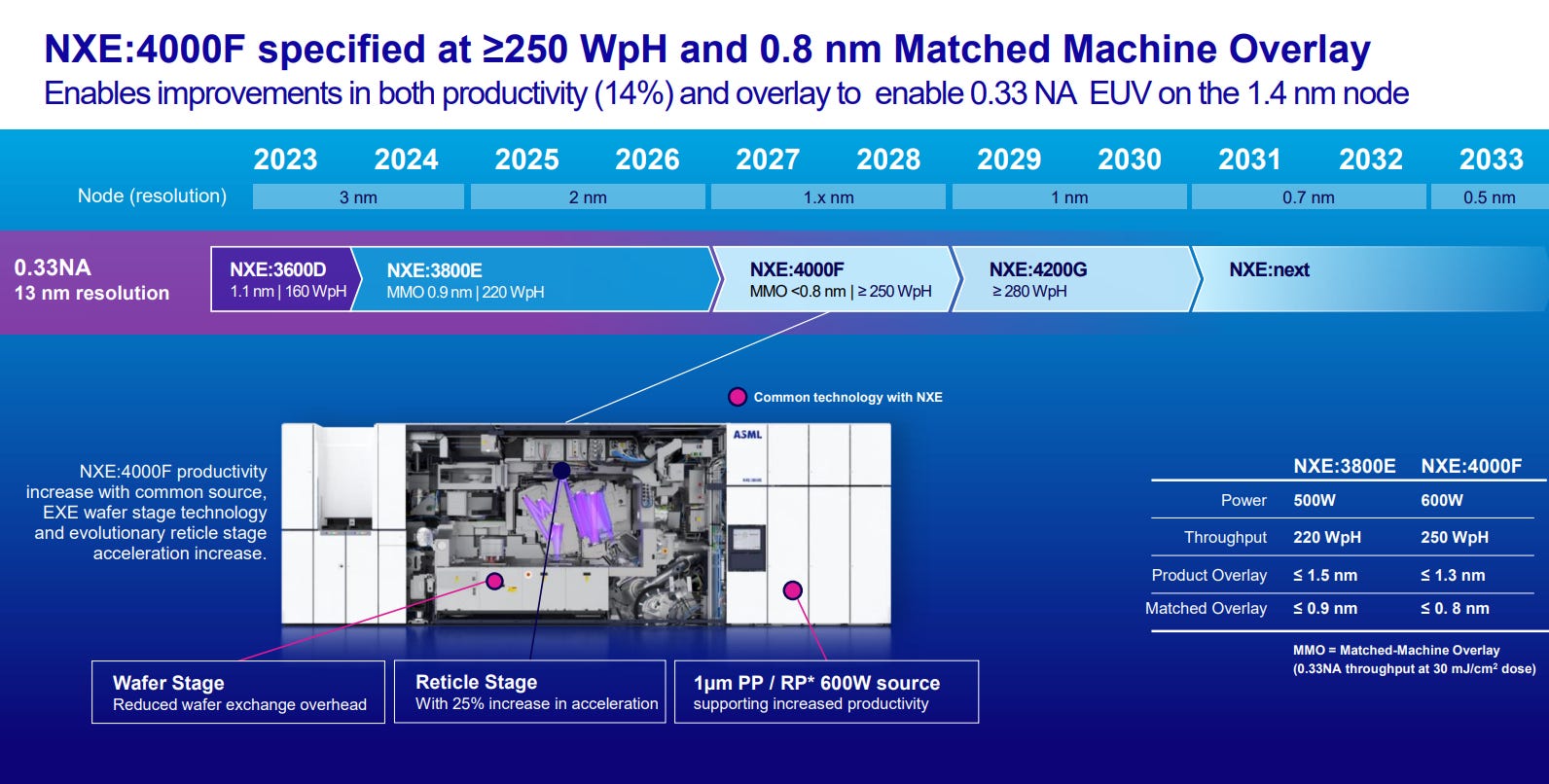
The second major issue is thermal stability. With the advent of new manufacturing nodes (2nm and smaller) and High-NA EUV technology, the power of lithography systems is pushing into the 500–600W range. At these levels, the pellicle heats up significantly. Combined with the brittleness of silicon, this leads to mechanical failure due to thermal expansion.
The semiconductor industry thus finds itself at a point where further power increases based on existing materials are physically unsustainable.
The choice is stark: either slow down the pace of technological development or find a new material capable of withstanding these extreme conditions long-term.
The Solution: Carbon
Canatu’s technology provides the answer to these physical limits. Remember the web made of smoke described earlier, comprised of 97% empty space? What looked like a laboratory curiosity is now the solution to a billion-dollar problem.
Canatu replaces the solid silicon layer with a porous network of carbon nanotubes (CNTs). Carbon is a material with extreme thermal resistance (withstanding temperatures over 1500°C), and thanks to its network structure, it can efficiently dissipate heat without deforming. The mechanical strength of the nanotubes solves the brittleness issue, while the high proportion of empty space (void fraction) ensures record EUV transmission that a solid material can never offer.
It sounds like the perfect solution. However, when looking at the material’s structure under a microscope, a new, seemingly logical concern arises for every physicist.
The Optical Paradox: Why Does the Web Cast No Shadow?
When imagining a network of carbon nanotubes, a very natural question may strike the reader: If there is a structure resembling a fine mesh in the optical path, why doesn’t its outline imprint onto the world’s most expensive chips and destroy them?
The answer lies in optics, specifically, in the depth of field (or depth of focus) of the lithography system. The protective pellicle does not sit directly on the photomask but is suspended several millimeters above it on a separate frame. This places it completely out of the focal plane of the EUV lithography machine.
A good analogy is taking a photo through a wire fence. If you focus your camera on a distant landscape, the fence, which is very close to the lens, practically disappears in the resulting image. It doesn’t vanish because it isn’t there, but because it is out of focus. The only effect is a slight reduction in the total amount of light hitting the sensor.
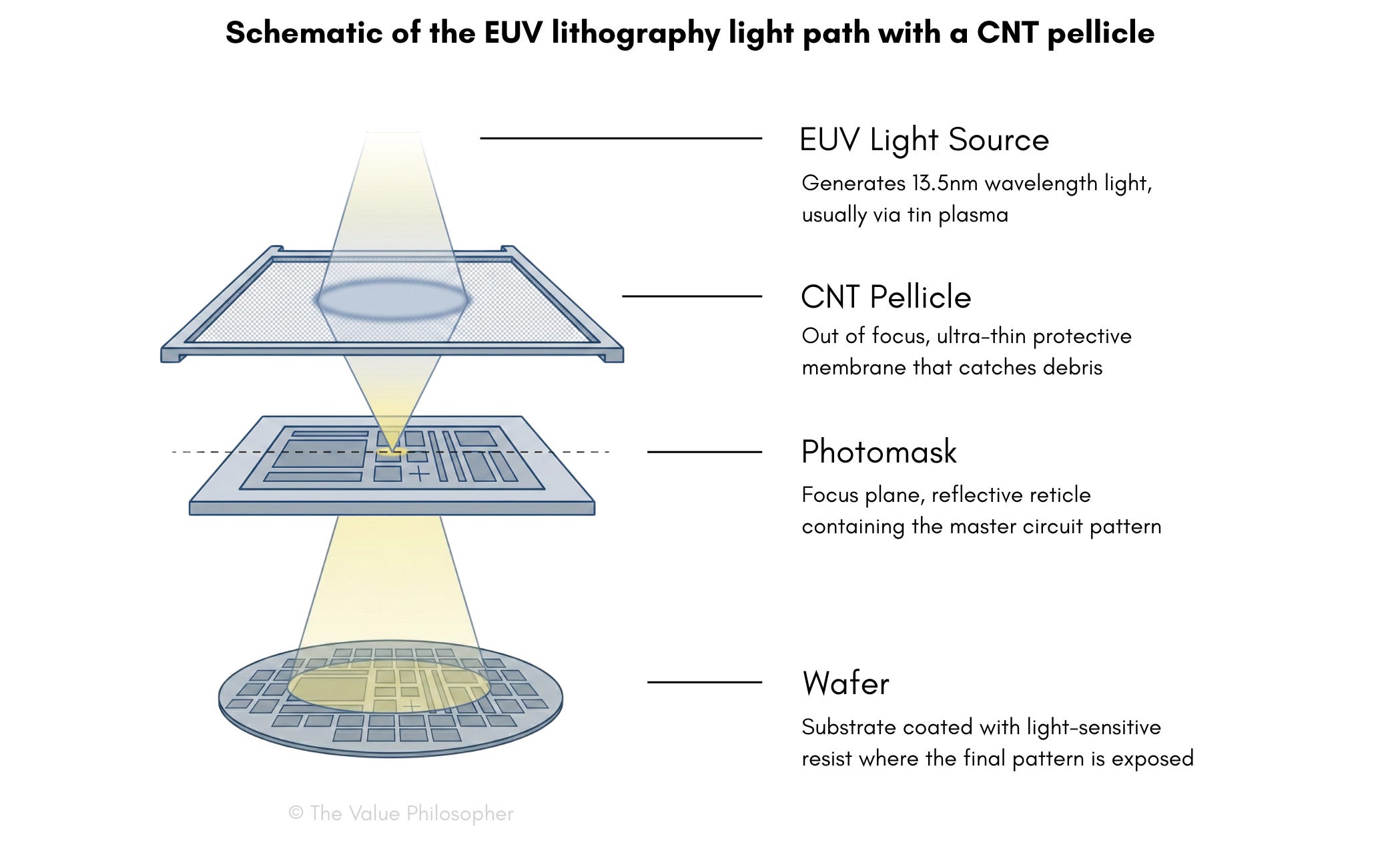
The same principle applies to EUV lithography. The pellicle projects no sharp image or shadow onto the chip structure. The only consequence of its presence is a certain attenuation of EUV intensity, meaning lower transmission. That is why transmission is one of the key parameters Canatu strives to maximize.
However, for this optical principle to work reliably at the nanometer scale, the pellicle must be extremely homogeneous. If it were denser in one area than another, it would cause local variations in light intensity (non-uniformity), which would manifest as defects on the wafer.
This is precisely where Canatu’s technological advantage shines. Their Dry Deposition process creates a statistically highly uniform nanocarbon layer. To the EUV scanner, this layer behaves like an optically uniform, clean medium, rather than an irregular structure.
ASML
For the two of you who don’t know ASML yet: it’s a Netherlands-based technology company specializing in the development and manufacturing of advanced lithography systems used in semiconductor fabrication. ASML is currently the world’s sole supplier of extreme ultraviolet (EUV) lithography tools and plays a critical, near-monopolistic role in enabling leading-edge chip manufacturing globally.
CNT Pellicles in ASML Roadmaps
Based on publicly available information, there are credible indications that ASML is preparing its EUV lithography platforms for compatibility with CNT-based pellicle technologies.
“If you take ASML’s published roadmaps, then CNT is included in this next NODE generation, and ASML has made certain optimizations to their devices to ensure that CNT performance is as good as possible in this next generation.“ - CEO Juha Kokkonen
This statement suggests that CNT pellicles are not merely an external materials innovation, but are increasingly being considered within the broader EUV ecosystem design, including tool-level compatibility and performance optimization.
Further support for this interpretation can be found in technical literature presented at SPIE conferences, including work on 0.33 NA EUV systems for high-volume manufacturing, which discusses evolving system requirements for mask protection, thermal stability, and exposure efficiency in advanced EUV environments.

Secret Partnerships: Reading Between the Lines
We operate in the world of manufacturing technology for the most desirable and expensive chips on the planet. Here, the rules of ordinary marketing do not apply. Amidst trade secrets and draconian NDAs (non-disclosure agreements), a thick fog of information reigns supreme. Companies announce nothing that might tip off the competition about which technology they are deploying.
In Canatu’s case, this shroud of secrecy is particularly dense. Official press releases avoid naming end customers, but there are enough hints left on the table to lead us to some very interesting conclusions.
The FST Partnership: A Direct Bridge to Samsung
One of the most frequent questions is: “Does Canatu supply directly to giants like Samsung?” The answer is typically corporately complex: “No, but actually yes.” To find it, we must follow the money and the ownership structures of their partners.
On October 23, 2025, Canatu announced a major milestone: it concluded a licensing agreement for the mass production of its pellicles with the South Korean company FST (Fine Semitech Corp). At first glance, this might seem like just another obscure name on a long list of subcontractors. However, a look at FST’s shareholder structure reveals a crucial detail: Samsung Electronics significantly invested in this very company in 2021, with the strategic goal of securing key components for its own semiconductor manufacturing.
A relatively straightforward equation emerges. Samsung needs new types of EUV pellicles for its advanced manufacturing processes, so it secures a capital stake. FST, in turn, needs the technology to manufacture these pellicles at an industrial scale, so it signs a licensing deal with Canatu and purchases their production reactors (more on those later). The result is that Canatu becomes a technology enabler in Samsung’s supply chain without having to figure as a direct supplier to the end customer.
From a business perspective, this is an extraordinarily efficient model. Canatu does not need to build capital-intensive manufacturing infrastructure in Korea, nor does it bear the logistical and operational risks. These are assumed by the licensing partner, while Canatu collects license fees and revenue from the delivery of know-how and reactors with significantly higher margins. FST thus functions as a strategic bridgehead between Canatu and Samsung.
“They (FST) have now reached the point where they wanted to buy this mass license... and everything is currently going, let's say, extremely well in the direction that we could start doing mass production in the near future.” - CEO Juha Kokkonen, 14.1.26
The Taiwanese Trail: Who Is the Mysterious Unnamed Customer?
If FST can be interpreted as an indirect route to Samsung, the key question remains: Who is this second customer that Canatu’s management speaks of only in hints, and with whom, according to public statements, advanced qualification tests are underway?
There is no official answer. Yet, when analyzing publicly available information, all relevant clues point to a single geographic and industrial hub: Taiwan.
Digital Footprints on LinkedIn
An interesting detail lies in Canatu’s own personnel structure. Although it is a relatively small Finnish firm with roughly a hundred employees, it has long maintained a senior commercial position directly in Taiwan, typically designated as a Sales Director or Key Account Manager.
Let’s ask a logical question: Why?
Why would a company of this size keep a high-level executive on an island on the other side of the world? The answer is readily apparent. There is only one customer in Taiwan whose size, technological significance, and future volumes justify such an investment: TSMC.
TSMC is the world’s largest and most technologically advanced chipmaker, and simultaneously the first company to introduce 2nm manufacturing nodes, precisely where the limits of existing pellicles are most glaring. The presence of a key sales representative directly in this environment strongly suggests that it is indeed TSMC serving as the second customer testing Canatu’s technology in the qualification phase.
CEO’s Words: Dominance Within Reach
Canatu’s CEO, Juha Kokkonen himself alluded to significant negotiations in a recent interview. When asked about cooperation with this second customer, he answered reservedly and diplomatically, yet the substance was crystal clear:
“These negotiations are not yet at a stage where we can disclose them. But let’s say that based on these talks, we are in a situation where, if they go well, we could secure a very dominant market position in the field of CNT pellicles.” - CEO Juha Kokkonen, 14.1.26
This statement is pivotal. A dominant position would not be achievable through cooperation with a fringe player. However, if Canatu already has indirect access to Samsung via FST and simultaneously secures TSMC as another key client, it would practically position itself as the technological standard for next-generation EUV pellicles.
“We have two significant semiconductor industry clients, both of them are from Asia. One is a leading semiconductor manufacturer, a real top manufacturer, and the other is a key Korean player.” - CEO Juha Kokkonen, 28.11.25, Investor Event 2025
This basically confirms this theory.
What About Intel?
That said, it is worth acknowledging an alternative interpretation. Given Intel’s unusually strong and early commitment to High-NA EUV lithography, there exists a plausible scenario in which another, currently unnamed customer could be a company with requirements similar to Intel’s.
Among leading-edge manufacturers, Intel is widely viewed as one of the players that may face the earliest and most acute need for next-generation pellicle solutions, particularly as High-NA tools transition from pilot operation to meaningful production use. In such an environment, CNT pellicles could shift from being a performance optimization to an operational necessity.
“I can say that this week, I won’t say which operator, but in a certain part of the world, a certain operator is making hundreds of wafers a day with the very latest ASML lithography devices, relying on Canatu’s CNT pellicle technology.” - CEO Juha Kokkonen, 14.1.26
Juha mentions the latest ASML lithography devices, which are currently owned by Intel, but also mentions hundreds of wafers a day, which would rather point towards TSMC. Until official disclosures or press releases clarify the matter, any attribution beyond a potential, unnamed customer remains speculative and should be treated with caution.
Anyway, how can a small firm from Finland supply giants like Samsung or TSMC with millions of pellicles without going bankrupt building factories?
This is where the genius of their business model comes in.
The Business Model: Scaling Technology Without Manufacturing Risk
So far, we have focused on the manufacturing technology, the pellicles themselves, and their indispensable role in the semiconductor industry. However, the fundamental question remained: how does Canatu intend to turn this technological advantage into a long-term sustainable and scalable business?
This is where an exceptionally well-thought-out and strategically robust approach reveals itself.
In the context of rising geopolitical tensions, shipping risks, and the drive by key players to maintain strategic control over production, typically TSMC, which deliberately keeps a substantial part of production directly in Taiwan, centralized manufacturing and global distribution of pellicles would represent a significant logistical and security burden.
Canatu has therefore chosen a different, significantly more elegant path.
Instead of custom-manufacturing pellicles and subsequently shipping them in large volumes to end customers, the firm opted for a model of decentralized manufacturing. It developed specialized equipment for pellicle production, which it calls a reactor, and delivers this reactor directly to its partners. They can then manufacture pellicles autonomously, directly within their own production facilities, in the exact quantities and timing that match their operational needs.
This approach significantly reduces logistical complexity, minimizes geopolitical risks, and simultaneously increases the solution’s attractiveness to customers.
The key element of this entire strategy is the fact that the delivery of the reactor marks only the beginning of the business relationship. Canatu has built a sophisticated business model around a single device that generates revenue from three mutually reinforcing channels.
Three Revenue Streams from One Box
I) Hardware Sales
The first stream is the sale of the hardware itself, specifically the CNT100 SEMI Reactor, which represents a one-off, yet volumetrically significant revenue injection from the delivery of the technological equipment.
II) Consumables
The second pillar is consumables. The reactor cannot function with commonly available gases or chemicals; it requires specific proprietary precursors and catalysts, the composition and production of which are fully controlled by Canatu. The partner is thus compelled to regularly purchase these materials directly from the technology manufacturer, creating a stable and recurring revenue stream.
III) Licensing Fees
The third and, from a margin perspective, most attractive revenue source is licensing. Canatu collects an agreed-upon amount for every single pellicle manufactured and sold. It doesn’t matter whether the partner produces thousands or millions of units, the company receives a share of sales from every product, without incurring any additional manufacturing or operational costs.
Margin Transformation
The result is a model that effectively transforms Canatu from a classic manufacturing firm into a high-margin technology licensor.
Manufacturing risk, capital intensity, and operational complexity are borne by the partner, while Canatu monetizes its know-how, patents, and technological dominance. This combination of a technological moat and a smart business model represents one of the strongest pillars of the company’s entire investment thesis.
In the context of future revenue, it is crucial to understand that an EUV pellicle is not a component that lasts forever. In the extreme environment of a lithography scanner, where light power in the order of hundreds of watts hits a membrane thinner than a human hair, accompanied by rapid pressure changes, it is a classic consumable.
Although Canatu’s CNT technology boasts vastly superior durability compared to older polysilicon solutions, in high volume manufacturing conditions, even it eventually wears out and must be replaced regularly.
For an investor, this finite lifespan is paradoxically key. It ensures that a single sold reactor must constantly produce new pellicles for its owner (e.g., TSMC). For Canatu, this generates a stable, long-term, and recurring stream of licensing royalties.
Scalability and IP Protection
The company’s strategic goal is to transition from a material supplier to a technology licensor, selling the reactors themselves while licensing the process to partners, whether they are chemical giants or semiconductor manufacturers directly.
This approach, however, raises a legitimate question for any rational investor:
If the firm sells its machine, isn’t it essentially providing the competition with a blueprint to bypass or destroy it? What stops engineers in China or Silicon Valley from tearing the reactor apart, analyzing it, and building their own clone?
The fundamental answer lies in the distinction between the physical hardware and the manufacturing process itself.
While the reactor represents physical infrastructure, a system of pipes, heating elements, sensors, and control units, Canatu’s real intellectual property is anchored in the process parameters of carbon nanotube production. These parameters cannot be fully derived simply by analyzing the equipment; they are software-controlled trade secrets.
This involves precisely defined gas flow conditions, pressure and velocity profiles, the management of laminar flow without turbulence, dynamic temperature changes in extremely short time intervals, and specific mixing ratios of precursors and catalysts. It is the combination of these factors that determines the resulting properties of the nanomaterial and its usability in nanometer-scale semiconductor applications. These process details are not accessible to the end customer and remain fully under Canatu’s control.
Practically speaking, the customer receives a functional manufacturing system whose output meets required parameters, but without the ability to reproduce the technology outside the scope of the licensing agreement. This approach significantly limits the risk of technology leakage, even in environments with highly sophisticated engineering teams.
The Supply Chain Ecosystem
The second key layer of protection is the structure of the market itself and the profile of the customers.
Canatu operates exclusively in a niche and highly regulated segment of the semiconductor ecosystem, where its partners are entities like TSMC, Intel, Samsung, or their direct suppliers. This market is characterized by extreme transparency, long-term contractual relationships, and strong legal protection of intellectual property.
Given the interconnectedness of the entire supply chain with ASML technologies, any attempt at illegal use or copying of the technology would be immediately detected within the supply chain. It would lead to legal battles, loss of market access, and catastrophic reputational damage. For global semiconductor leaders, whose business relies on long-term trust, regulatory compliance, and capital-intensive infrastructure, such a risk represents economically unacceptable behavior.
The combination of software-driven process know-how, patent protection, a licensing model, and an exclusive, highly regulated market creates a robust defensive mechanism. This framework allows Canatu to scale its technology efficiently without jeopardizing its competitive position, supporting the company’s transition toward a high-margin, capital-efficient deep-tech model.
Modeling Future Pellicle Demand
As part of this in-depth analysis, I considered it useful to examine the broader context of contemporary semiconductor manufacturing. This section will be very mathematical, quantitative and data-driven, readers primarily interested in the conclusions may want to skip ahead.
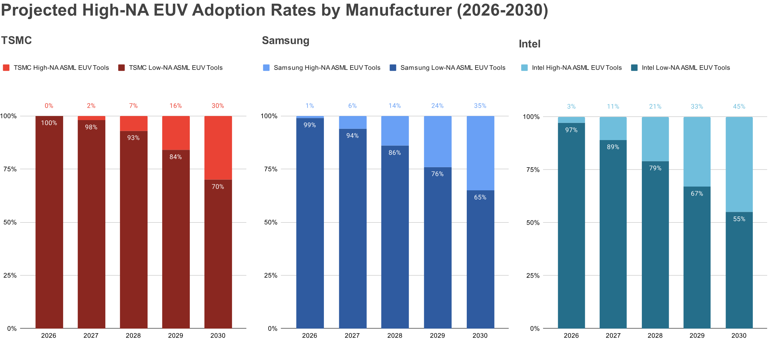
I constructed a table capturing the current scale of operations of the three leading logic semiconductor manufacturers: TSMC, Samsung, and Intel.
Based on publicly available roadmaps and forward-looking plans, I subsequently developed a second table projecting the situation in 2030. This projection reflects the anticipated gradual transition from Low-NA EUV lithography systems to High-NA EUV systems supplied by ASML. It is important to emphasize that this transition is expected to be slow and incremental, rather than abrupt.
In addition to tool deployment, the tables also illustrate production intensity, expressed as monthly wafer output, along with the estimated percentage split of production between Low-NA and High-NA EUV systems. For the year 2030, this percentage distribution is necessarily an estimate, derived from currently available information and industry signals. It should therefore be understood as an indicative scenario rather than a precise forecast, and actual outcomes may differ materially.
The primary motivation for this modeling exercise is not to predict exact future outcomes, but rather to establish a structured baseline and analytical reference point. This framework serves as a conceptual starting platform for evaluating potential scenarios in the semiconductor manufacturing segment, particularly in relation to downstream implications for EUV-related consumables such as pellicles.
Main Data Sources
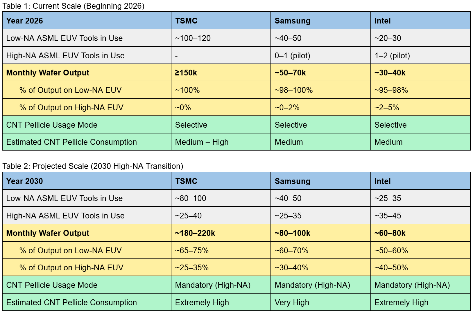
As shown in the tables above, a gradual increase in wafer production processed on High-NA EUV systems can be observed over time. As previously noted, however, the adoption of High-NA EUV is expected to be incremental rather than rapid. In the case of TSMC, it is therefore reasonable to assume that Low-NA EUV systems will remain the dominant production platform even in 2030, particularly given TSMC’s traditionally conservative, yield-focused approach to process transitions.
By contrast, Intel’s early and explicit strategic commitment to High-NA EUV positions the company to potentially become a leader in High-NA-enabled manufacturing over the longer term. This strategic positioning may partly explain the company’s recent positive market sentiment, reflected in a significant appreciation of its share price over the past month, although equity performance should of course be interpreted cautiously and in a broader context.
A further important observation concerns the role of CNT pellicles. While today the adoption of CNT pellicles can still be considered largely optional and selective, particularly under Low-NA EUV operation, this situation changes fundamentally with the introduction of High-NA EUV. Under High-NA conditions, CNT pellicles transition from a discretionary optimization to a functional necessity, driven by increased thermal load, higher exposure intensity, and stricter mask protection requirements. As a result, pellicle consumption is expected to increase substantially by 2030, not only due to higher tool counts, but also because of shorter pellicle lifetimes and higher replacement frequencies.
CNT Pellicles and Energy Efficiency
It is also important to note that, although TSMC’s adoption of High-NA EUV systems is relatively gradual, CNT pellicles could be introduced at any stage of this transition not solely due to technological necessity, but also because of their intrinsic performance advantages. Even under Low-NA EUV operation, CNT pellicles offer superior characteristics, such as higher EUV transmission, which can translate into meaningful efficiency gains.
Given that TSMC operates the largest installed base of ASML EUV systems, its aggregate energy consumption associated with lithography is substantial. In this context, the use of CNT pellicles could contribute to reduced energy losses per exposure, potentially delivering non-trivial efficiency improvements at scale. As a result, the implementation of CNT pellicles may be economically and operationally attractive even on Low-NA EUV tools, independent of High-NA-driven requirements.
Pellicle Consumption Modeling Framework
Based on the data presented in the preceding tables, I derive a single, generalized equation that serves as a transparent approximation of CNT pellicle consumption. The purpose of this formulation is not to model fab-level behavior with high precision, but rather to explicitly link production scale, EUV process complexity, pellicle lifetime, and CNT adoption into a coherent analytical framework.
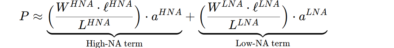
Where:
W = wafers / month
ℓ = EUV layers per wafer
L = pellicle life in wafer-layer equivalents
a = CNT pellicle adoption rate (share of EUV layers actually using CNT pellicles)
HNA = High-Numerical-Aperture (High-NA) EUV lithography systems
LNA = Low-Numerical-Aperture (Low-NA) EUV lithography systems
Model Assumptions And Scenarios
The parameters below, in Table 3 provide the input assumptions required to estimate CNT pellicle consumption under different technology adoption pathways. To better capture the uncertainty inherent in long-term semiconductor roadmapping, I structure the outlook into three scenarios.
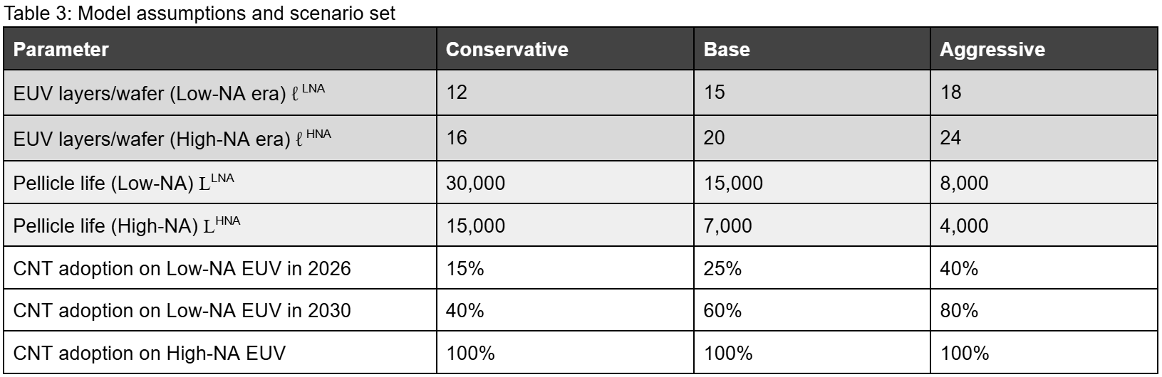
The conservative scenario represents a lower-demand outcome, driven by a smaller number of EUV layers per wafer, which implies lower exposure intensity and longer pellicle lifetime, combined with a slower and more limited rate of CNT pellicle adoption, particularly under Low-NA operation.
The base scenario reflects a mid-range trajectory consistent with gradual High-NA ramp, increasing EUV layer counts, and moderate CNT adoption. For the base scenario, a pellicle lifetime of approximately 15,000 exposure cycles was assumed, as this value is commonly cited in industry discussions and reflects the generally accepted order of magnitude for current-generation EUV pellicle durability under standard operating conditions.
Finally, the aggressive scenario captures a higher-demand outcome characterized by a larger number of EUV layers per wafer and therefore higher exposure intensity, which in turn implies shorter pellicle lifetime and higher replacement frequency, alongside faster and broader CNT adoption across EUV layers.
Scenario-based modeling is particularly appropriate in this context due to the limited availability of publicly disclosed, quantitative data on EUV tool utilization, pellicle lifetime, and mask-related consumable usage at leading-edge nodes. In addition, the transition toward High-NA EUV is subject to significant uncertainty, influenced by factors such as tool delivery schedules, yield learning curves, process integration challenges, and company-specific technology strategies.
As a result, any single-point forecast would risk conveying a false sense of precision. The use of multiple scenarios therefore provides a more robust and transparent framework, allowing a structured exploration of plausible outcomes while explicitly acknowledging the underlying uncertainties.
Modeling Methodology
To operationalize the forecast model, I converted the estimated production ranges into discrete midpoint values for calculation.
For the 2026 baseline, I pinned Samsung and Intel to the exact arithmetic means of their estimated capacity (60k and 35k WPM, respectively) and set TSMC at 160k WPM; a representative figure just above the 150k floor.
For the 2030 High-NA transition, I applied the precise midpoints of both the wafer output and High-NA market share projections: 200k WPM for TSMC (30% High-NA), 90k for Samsung (35% High-NA), and 70k for Intel (45% High-NA).
These standardized inputs provide a deterministic basis for the consumption formula, eliminating the ambiguity of overlapping variance ranges while remaining central to the forecasted trends.
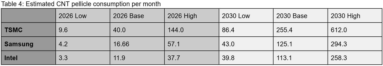
Model Results
Based on the input data in Table 1 (2026 baseline) and Table 2 (2030 projection), and using the scenario assumptions defined in Table 3, we apply the model equation to derive a first-order estimate of CNT pellicle consumption today versus 2030. Here are the results of the estimated pellicle monthly consumption:
Or to make this data annualized for better clarity, using the base scenario only:
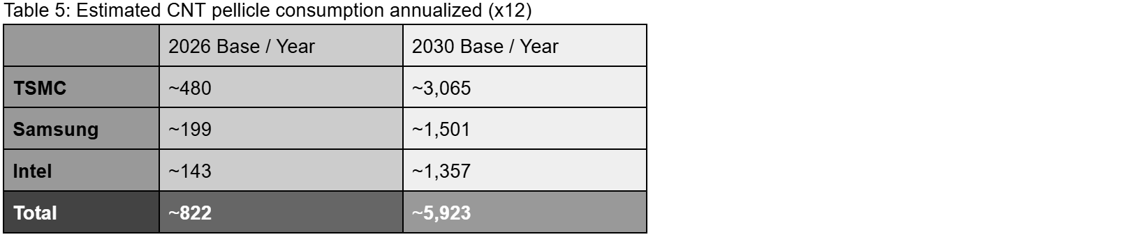
The combination of High-NA EUV adoption and increasing process complexity implies a pronounced increase in pellicle demand. Under the assumption that CNT pellicles become the industry standard, the model indicates that total annual consumption across the three manufacturers increases from approximately 822 pellicles per year in 2026 to approximately 5,923 pellicles per year in 2030 (base scenario).
This corresponds to an increase of about +620%, i.e., roughly a 7.2× growth in estimated annual pellicle consumption.
Feel free to use the model and equations presented here with your own data assumptions. In this analysis, I intentionally chose lower-end estimates, favoring a more cautious and downside-oriented scenarios. This approach reflects a preference for stress-testing the model rather than assuming optimistic outcomes.
Visual Analysis
To make the results easier to understand, I decided to take the output of the model and present it through a set of visualizations. It’s important to keep in mind that all of these results sit firmly within the boundaries of the model itself. I therefore focus exclusively on leading-edge logic manufacturing that is critical for future workloads, considering only three main companies: TSMC, Samsung, and Intel.
For that reason, the global demand for CNT pellicles may differ significantly from the figures shown here, which should be interpreted as a focused subset rather than a complete view of the overall market.
This chart illustrates the projected adoption of High-NA EUV lithography tools across all three manufacturers. Using the adoption ratios defined in Table 1 and Table 2, I interpolate the intermediate years (2027–2029), while keeping the 2026 and 2030 boundary assumptions unchanged.
The resulting trends are consistent with the broader industry narrative. TSMC appears to adopt High-NA more cautiously, while Intel moves significantly faster, reaching a point where nearly half of its wafer output in 2030 could originate from High-NA EUV tools. Samsung follows a more gradual but steady adoption path in between.
The combined estimate suggests that by 2030 only around one-third of total wafer output (~34%) across the three companies is produced using High-NA EUV tools, reinforcing the view that Low-NA EUV remains the dominant exposure platform well into the next decade.
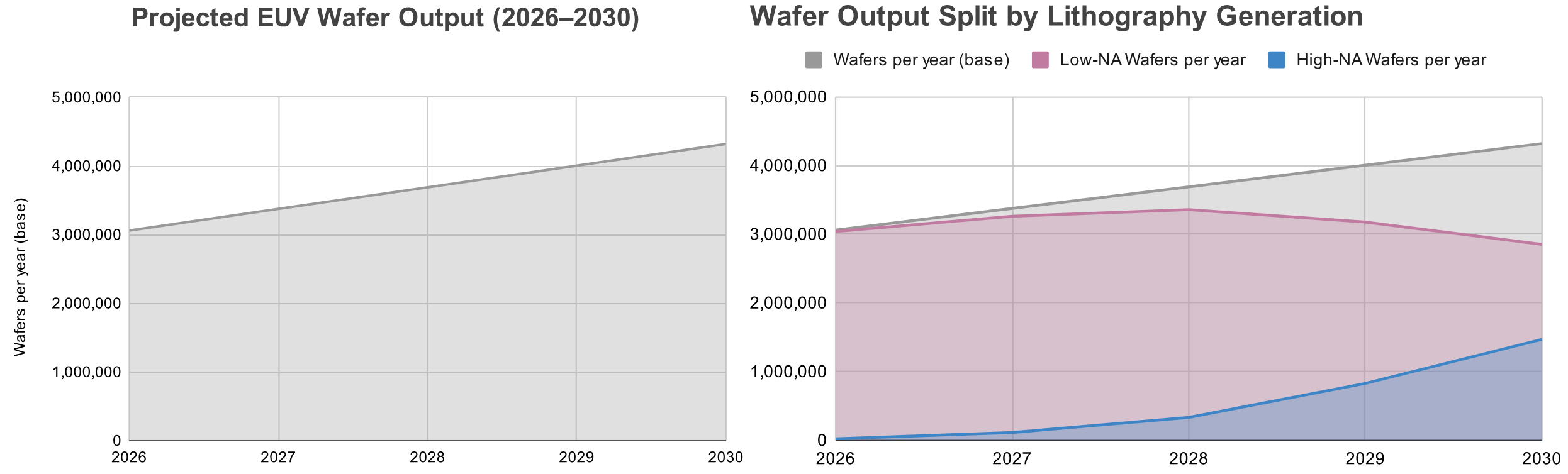
These two charts compare the steady scaling of total addressable wafer volume against the dynamic shift in manufacturing technology. As visualized in the split analysis (right), 2028 marks a noticeable turning point, where High-NA momentum visibly accelerates, transitioning from a pilot niche to a substantial wedge of production.
However, despite this rapid uptake, the breakeven year, where High-NA wafer volume officially surpasses Low-NA volume, is not expected to occur within this decade. Based on the present growth trajectory, with High-NA gaining roughly 13 percentage points of share per year, the crossover where High-NA becomes the dominant volume driver is projected to occur around 2032 to 2034.
Now it gets a bit interesting. This forecast highlights a fundamental decoupling between wafer production and pellicle consumption, driven by the operational intensity of next-generation lithography.
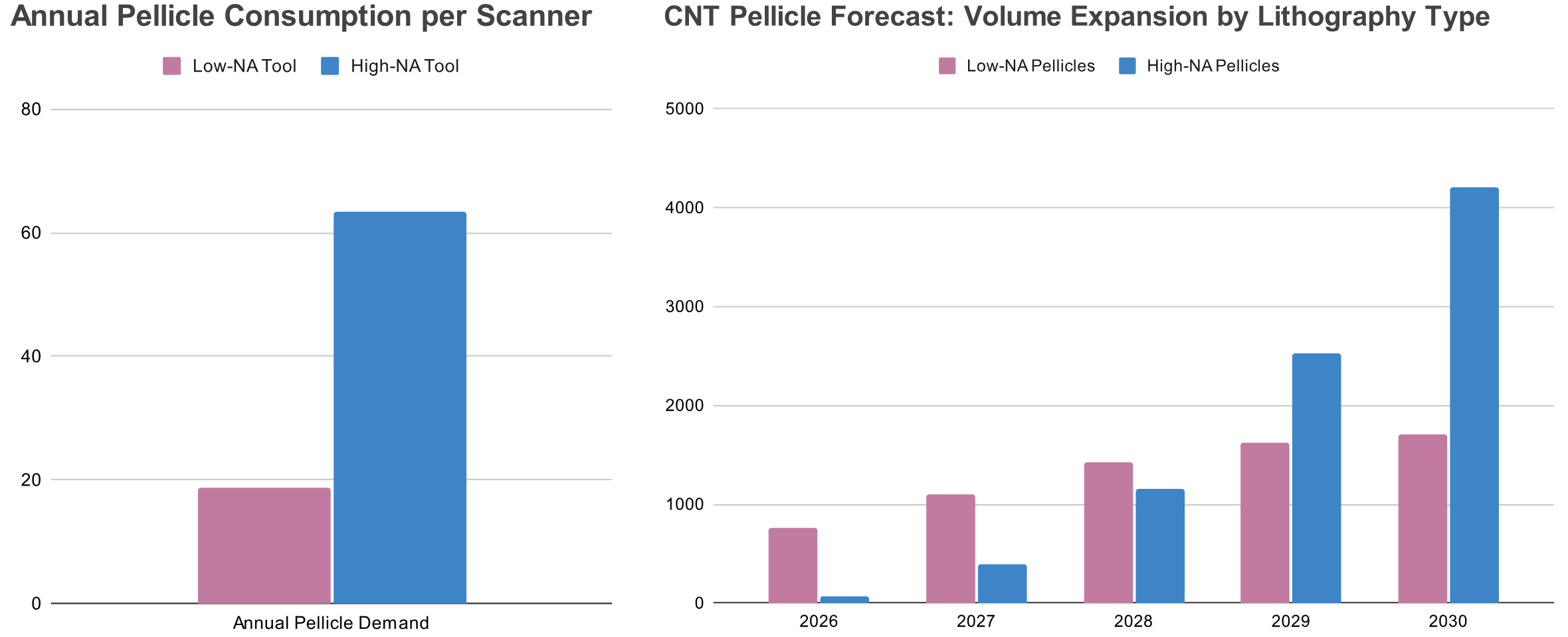
While High-NA scanners are projected to process only around 34% of total wafer volume by 2030, as mentioned earlier, my model indicates that they could account for more than 70% of aggregate CNT pellicle demand.
This imbalance is driven by a roughly 3.4× higher pellicle burn rate on High-NA tools compared with Low-NA systems. In practical terms, a single High-NA tool consumes pellicles more than three times faster.
This effect is the result of three compounding factors: significantly lower pellicle lifetime due to higher thermal loads (a 2.14× effect) and increased layer counts per wafer (an additional 1.33× multiplier).
As a result, from the perspective of the pellicle supply chain, the strategic importance of High-NA lithography far exceeds its share of total silicon output. Even as a minority contributor to wafer volume, High-NA emerges as the dominant driver of future pellicle demand.
Burn Rate Disclaimer
It is important to clarify that the projected 3.4x burn rate is a theoretical estimate derived from my model’s assumptions rather than publicly released operational data from ASML or major foundries. There is currently no public data that directly quantifies pellicle lifetimes on High-NA versus Low-NA EUV tools; however, the underlying physics of the transition strongly suggests a substantial increase in consumption.
A more precise calculation would require a real-world operational model, with proprietary inputs, such as specific source power duty cycles, thermal-cycle fatigue limits, and exact fab-level layer routing policies, that remain trade secrets. Therefore, while my model tests a high-stress scenario (3.4x), it is plausible that as CNT materials mature and thermal management strategies are optimized, this consumption multiplier could settle closer to a 2x factor.
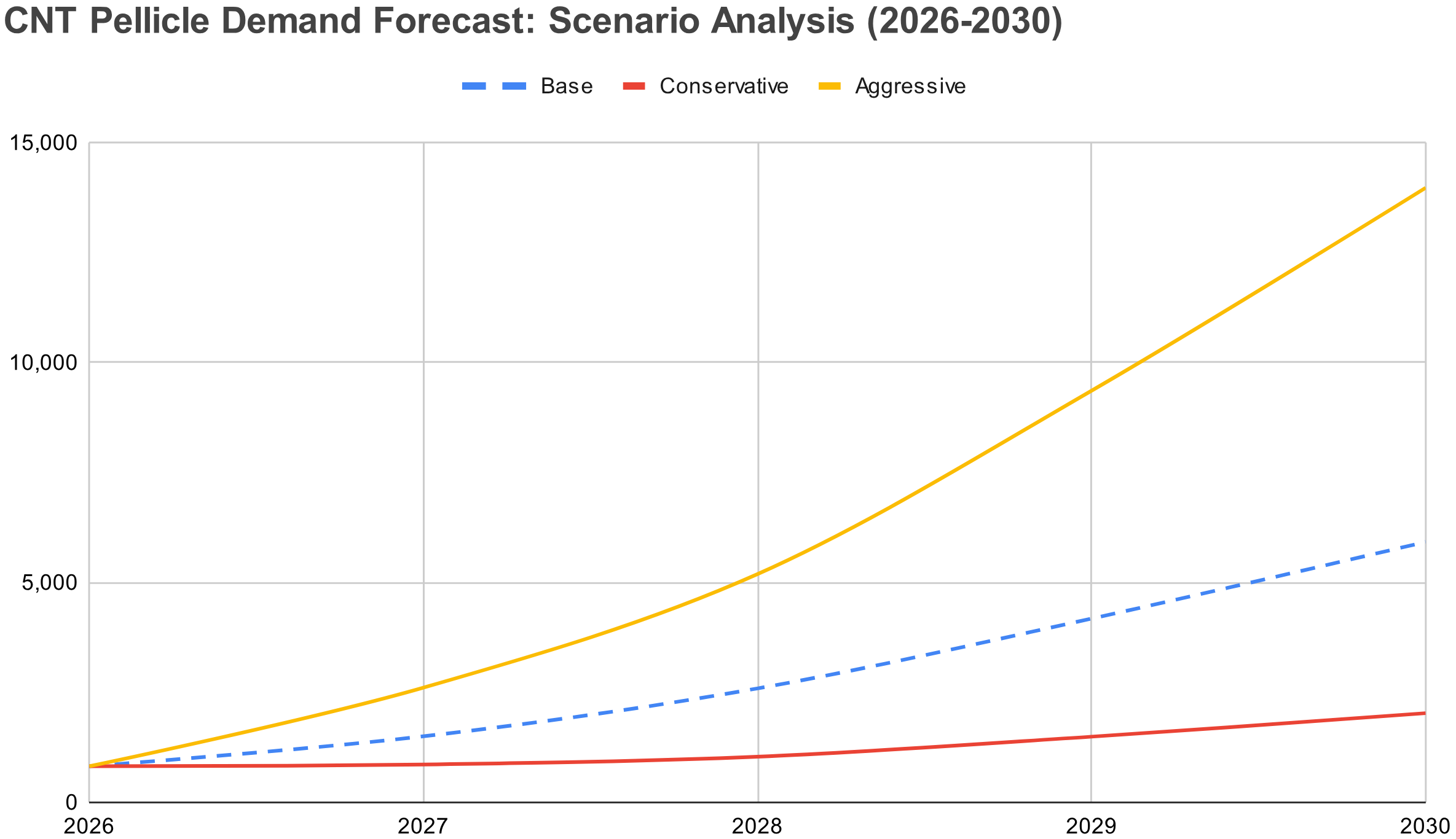
This last chart visualizes CNT pellicle demand across conservative, base, and aggressive scenarios, revealing a growth trajectory that is distinctly exponential rather than linear. This acceleration is driven by the fundamental shift in consumption intensity associated with next-generation lithography. In simple words, each additional High-NA scanner brought into operation contributes to higher overall pellicle demand.
DRAM Considerations
The pellicle consumption model presented in this analysis is intentionally focused on leading-edge logic manufacturing at TSMC, Samsung, and Intel, where pellicle demand is primarily driven by EUV layer complexity, High-NA adoption, and reduced pellicle lifetime under higher exposure intensity. Memory manufacturing, particularly DRAM, follows a structurally different lithography paradigm, characterized by fewer EUV layers per wafer, higher reticle reuse, and substantially larger and more homogeneous wafer volumes.
As a result, pellicle consumption dynamics in DRAM fabs are governed less by per-wafer EUV intensity and more by cumulative reticle exposure count and throughput-driven wear mechanisms, which are not explicitly captured in the present model.
Under scenarios where EUV adoption in DRAM accelerates materially toward the end of the decade and CNT pellicles become a preferred or mandatory solution due to thermal and durability requirements, it is plausible that DRAM could account for a significant share of total EUV pellicle demand.
Some industry estimates suggest that, in such a volume-driven wear regime, DRAM-related pellicle demand could approach ~30–40% of the total EUV pellicle addressable market by 2030.
This outcome should be interpreted as an upside scenario rather than a base case and is presented here to highlight the potential contribution of memory manufacturing beyond the logic-centric framework analyzed above.
The Future Will Tell
That said, who knows how many pellicles will be actually needed in 2030?
It is important to note that CNT pellicles may find adoption well beyond leading-edge logic manufacturers. As mentioned above, potential users could include memory-focused semiconductor companies, such as SK hynix, Micron, and others.
As with most transitions in semiconductor manufacturing, the eventual outcome will likely emerge gradually, shaped by practical experience rather than by any single forecast.
Pricing Context and Market Implications
The current market price of conventional silicon-based EUV pellicles is generally estimated to lie in the range of approximately USD 15,000–25,000 per unit, based on industry reports and technical market analyses. These pellicles are designed for Low-NA EUV operation and are subject to material and thermal limitations that become increasingly pronounced as process complexity rises.
With the transition toward High-NA EUV lithography and more demanding exposure conditions, it is reasonable to assume that CNT-based pellicles will command a higher price point. Despite their superior mechanical and thermal resilience, CNT pellicles rely on more advanced materials, tighter manufacturing tolerances, and proprietary processes.
Under these assumptions, the addressable annual market for CNT pellicles in 2030 appears highly attractive, as you can do the math yourself here. Given the modeled increase in pellicle consumption driven by High-NA adoption and higher replacement frequencies, and assuming CNT pellicles become the industry standard, the resulting market opportunity scales rapidly.
More about EUV pellicles, their lifetime and updated information in:
PART 2: CNT Pellicles Explained: Hydrogen, Lifetime, and the Demand Math
China and Competition
Every investor naturally asks the same question in cases like this:
If this is European technology, what stops China from simply replicating it within a year and manufacturing it for half the price?
In Canatu’s case, however, this often-cited scenario hits two fundamental barriers that make rapid and cheap Chinese competition highly unlikely.
We have already discussed their Dry Deposition method. Canatu allows for the creation of nanotubes directly from the gas phase, without any contact with liquids. This process preserves the material’s structural integrity and achieves parameters necessary for the most advanced applications. Moreover, the entire procedure is protected by more than 213 patents, creating an exceptionally strong technological and legal moat.
The Geopolitical Wall
The second, and perhaps even more critical barrier, is the geopolitical context of the current semiconductor industry.
Even in the hypothetical scenario where Chinese firms managed to bypass or copy this technology, they would hit a fundamental practical problem:
They would have nowhere to use it.
The membranes developed by Canatu are designed exclusively for the most advanced EUV lithography machines manufactured by ASML. These machines are subject to a strict export embargo by the United States and the Netherlands, preventing China from purchasing them. Chinese companies, therefore, can neither develop nor test components for a system they do not physically own, and in all likelihood, never will.
Patents vs. Trade Secrets
When looking closely at Canatu’s patent portfolio, it is important to recognize the natural innovation cycle typical of deep-tech companies.
Although the original foundational patents from 2005–2008, protecting the very core of the technological principle, are gradually expiring between 2025 and 2028, this fact does not pose a major risk to the investment thesis. Protection is seamlessly shifting to newer application patents focused on specific industrial implementations, such as EUV pellicle structures or specific membrane designs, whose validity extends well into the coming decades.
However, an even more significant role is played by manufacturing know-how, the body of process knowledge and practical experience that is not, and cannot be, fully captured in patent documentation.
While a patent formally describes what is to be made, trade secrets protect how to fine-tune thousands of subtle manufacturing process parameters so that the resulting material meets the extreme demands of industrial applications. Unlike patents, this know-how never expires, and without mastering it, even publicly available technology remains practically very difficult, if not impossible, to replicate.
Mitsui Chemicals: The Established Giant
In the context of EUV pellicles, Mitsui Chemicals undoubtedly deserves mention. This major Japanese chemical group has worked closely with ASML for years and ranks among the main suppliers of traditional silicon EUV pellicles used in the current generation of lithography equipment. Today, Mitsui is likely the largest producer of these conventional pellicles and is fully in the system as a licensed and trusted supplier for the most advanced semiconductor manufacturing lines.
The company is consistently listed among key players in the global EUV pellicle market, alongside other major materials firms such as Shin-Etsu in the field of conventional solutions.
Mitsui Chemicals is also a significantly diversified company with a broad portfolio including performance and basic chemicals, polymer materials, films and sheets, engineering plastics, specialty chemicals, and materials used in electronics, the automotive industry, agriculture, consumer goods, and other segments. It operates globally, with manufacturing and research capacities in Japan, Asia, Europe, and the United States.
Compared to Canatu, it is an industrial titan with a market capitalization of approximately $5 billion, roughly fifteen times the value of Canatu, and possessing corresponding financial backing, R&D budgets, and institutional stability.
The IMEC Partnership and Mass Production
In December 2023, Mitsui announced a strategic partnership with the research hub IMEC, which serves as a shared technological platform for key semiconductor players, including Intel, TSMC, and Samsung. Through this collaboration, Mitsui aims to commercialize CNT membranes developed within the imec environment, effectively establishing a “standard” academic-industrial CNT pellicle solution.
Subsequently, in May 2024, the company announced the construction of a manufacturing plant for the mass production of CNT pellicles at its Iwakuni-Ohtake Works in Japan, with a planned capacity of approximately 5,000 units annually and a launch targeted around the end of 2025.
As of early 2026, I did not manage to find any updated information about the launch or operational status of this manufacturing facility.

Technological Differences
From a technological standpoint, however, Mitsui’s approach to CNT pellicle production differs fundamentally from Canatu’s dry deposition method described earlier. Mitsui builds on its long-standing experience with conventional photomask membrane production, utilizing CNT films prepared via solution-based or hybrid processes. These processes typically involve synthesizing nanotubes on a substrate, subsequently transferring them to a supporting membrane, integrating them into a frame, and final assembly in centralized manufacturing plants.
It is precisely this transfer step that is a known source of defects, contamination, and variability in CNT technology. In contrast, Canatu’s dry deposition technology eliminates this step entirely, nanotubes are deposited directly onto the frame without intermediate stages.
Evolution vs. Revolution
Although Mitsui’s approach is fully compatible with existing manufacturing infrastructure and supply chains for the pellicle industry, it inherently involves more handling and process steps. Each of these increases the demands on contamination control, uniformity, and yield. Mitsui’s CNT pellicles can thus be understood as an evolution of established manufacturing methods, whereas Canatu’s solution represents a fundamentally new paradigm designed from the very beginning for the extreme requirements of EUV and, specifically, High-NA lithography.
Centralized vs. Decentralized
From a business perspective, the difference is also evident in the scaling model itself. Mitsui manufactures pellicles centrally and ships finished products to mask-shops, fabs, and partners within the ASML ecosystem.
This model is well-known and comfortable for large semiconductor players, yet it carries the risks of centralized production bottlenecks, longer supply chains, and limited flexibility during sudden surges in demand. Conversely, Canatu offers not only the pellicles themselves but also a reactor and licensing model, enabling more decentralized and potentially faster production scaling closer to the point of consumption.
Mitsui Chemicals’ broad diversification undoubtedly provides it with stability, scale, and industrial reach that can aid its pellicle business. However, it also means that CNT pellicles represent merely one of many product lines that must compete for capital, management attention, and strategic priority. This can be an advantage in some respects, but also a limitation in a segment where physical limits and technological purity begin to play the dominant role.
The Bear Case: No Pellicle Dream
For a balanced view, we must address the most significant theoretical risk to this thesis, which is not a competition, but ASML itself. For years, the industry’s holy grail was to run EUV scanners completely naked, without any pellicle at all. The logic was simple, even the best membrane blocks some light, and in EUV lithography, photons are precious. ASML spent years attempting to shield photomasks using only high-pressure air curtains to blow away contaminants.
However, as the industry transitions to High-NA EUV, this dream has largely collided with economic reality. With source power pushing toward 600W and feature sizes shrinking to the angstrom scale, the risk of a single microscopic particle landing on a photomask is simply too high. A single speck of dust can destroy the yield of an entire wafer lot. The industry has effectively conceded that the cost of naked exposure (constant mask cleaning, inspection downtime, and yield risk) far outweighs the light loss from a high-transmission pellicle.
Crucially, as we confirmed earlier, ASML’s active optimization of their next-generation scanners specifically for CNT performance serves as the final nail in the coffin for the no pellicle bear case.
3. Medicine and Diagnostics
Alongside the automotive and semiconductor sectors, Canatu is systematically cultivating a third area of its business. While currently in an earlier phase, it holds high transformational potential: medical diagnostics.
Here too, the company leverages the key properties of its nanocarbon material, specifically the exceptionally large active surface area and the high electrochemical sensitivity of carbon nanotubes. These characteristics make them an ideal foundation for next-generation biosensors.
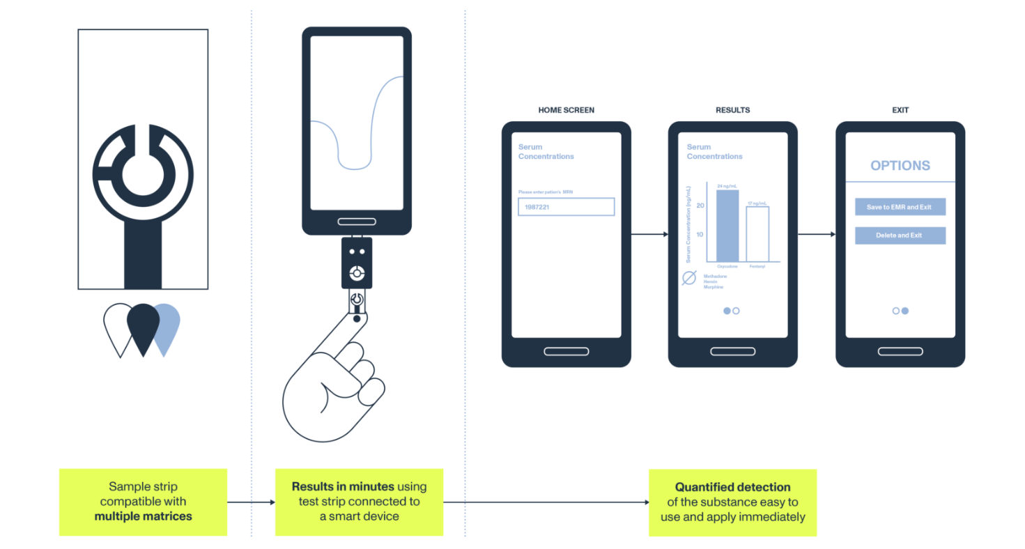
The strategic goal is to transfer laboratory-grade accuracy directly into ambulances and general practitioners’ offices, entering the realm of point-of-care (POC) diagnostics.
From this perspective, the current market state is unbalanced. Rapid field tests often suffer from low accuracy, while reliable laboratory examinations require logistics, time, and waiting periods measured in days. Canatu’s technology aims to bridge this gap.
CEO Juha Kokkonen has repeatedly stated that internal tests are already achieving results comparable to hospital laboratories, with validation conducted in collaboration with HUS (Helsinki University Hospital) among others. The fundamental difference lies in the time-to-result: instead of days, the analysis is available in minutes.
The company is currently increasing investments in this segment, focusing on the detection of specific biological markers such as hormonal levels (e.g., testosterone) or selected tumor markers. Although this area is still in the development phase and more detailed information will be presented at the upcoming Capital Markets Day, it already indicates that Canatu’s technology platform possesses potential far beyond purely industrial applications.
Financials and Management
Canatu is a relatively small company focused on developing new technologies. For understandable reasons, such companies typically post poor financial results in their early stages due to heavy operating expenses, including R&D salaries, material purchases, and the like. Even with rising revenue, seeing the financial situation stabilize takes time before profits settle enough to cover all operational costs.
Therefore, there is no point in dissecting sophisticated metrics and forecasts here. I obtained a digital copy of Canatu’s financials from a platform similar to the SEC. The data confirms reality: Canatu is undergoing a massive transformation from an R&D lab into an industrial manufacturer. I would like to review the financial basics here to give us a better idea of what the company is investing in, and so on.
Revenue Growth: Validating the Semiconductor Thesis
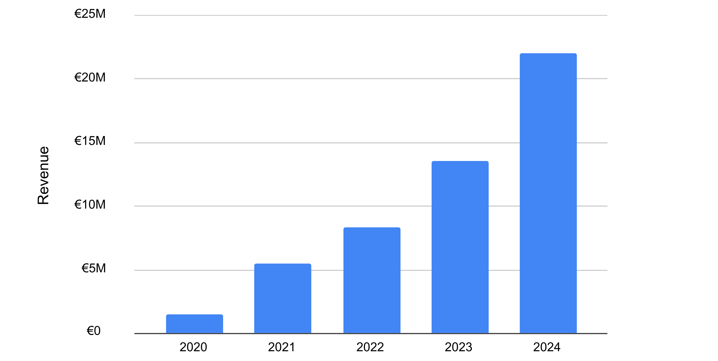
If anyone in the past doubted that Canatu’s future lies primarily in the semiconductor industry, the 2024 numbers have effectively ended those debates.
Total revenue grew by a significant 62.1% year-over-year (YoY), reaching €22.0 million, compared to €13.6 million in 2023. This growth was not broad-based but unequivocally driven by a single segment, semiconductors.
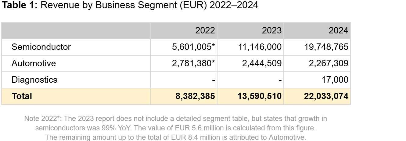
The semiconductor segment recorded literally explosive growth. Revenue here surged by 77.2% to €19.7 million, and it now constitutes the overwhelming majority of the company’s total income. Deliveries of CNT100 SEMI reactors and related projects for global chip manufacturers show that Canatu is successfully moving from the technological development phase to real commercialization.
Profitability: The Price of Aggressive Growth
As with most fast-growing deep-tech companies, revenue growth at Canatu does not yet translate to profitability. The firm remained in the red in 2024, which is an expected rather than a negative surprise at this stage of development. EBITDA ended the year in negative territory at −€2.5 million, and the net loss reached −€5.0 million.
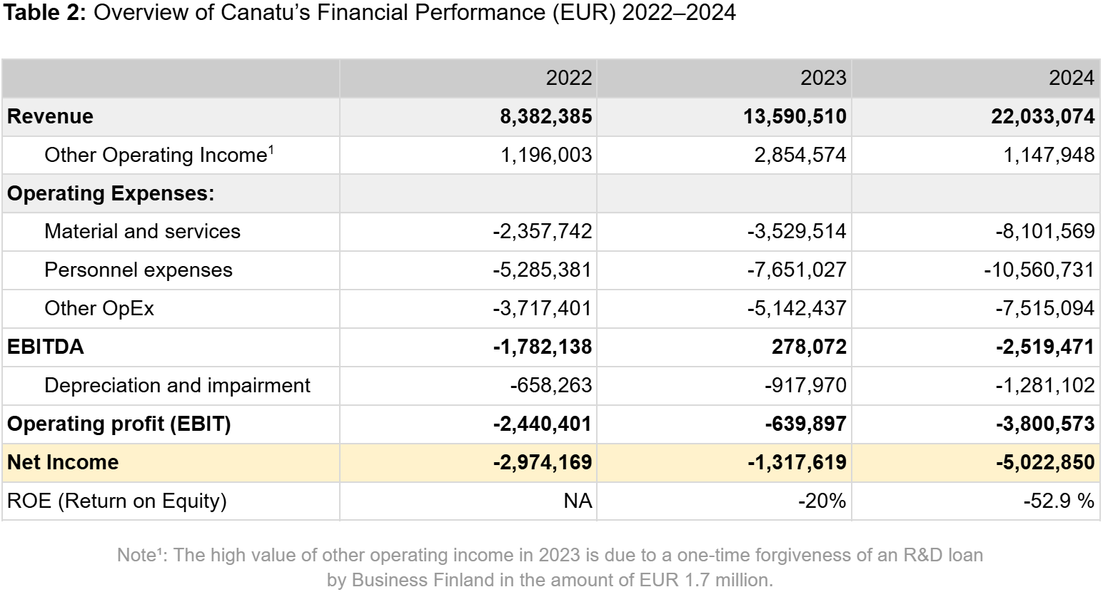
At first glance, it might seem paradoxical that a firm with over 60% revenue growth is still losing money. The answer lies in scaling costs. During the year, Canatu significantly expanded its team, headcount grew from 109 to 137, while massively investing in development and manufacturing capacity preparation.
A significant and often overlooked detail is the accounting treatment of R&D. The company does not capitalize R&D costs into assets but expenses them directly. In 2024 alone, €4.3 million in R&D expenses flowed directly into the P&L. This conservative and clean approach means the company isn’t artificially dressing up its results and transparently shows the true economic reality of its growth.
Where is the Money Going? CAPEX and Infrastructure Building
A look at investments and the balance sheet clearly shows that Canatu is not preparing for short-term profit optimization, but for a much bigger game. In 2024 alone, the company invested a total of €5.0 million in fixed assets. These funds did not go into marketing or administrative comfort, but primarily into physical manufacturing infrastructure.
Key investments included the construction of a new automated production line and the establishment of an ISO3 cleanroom, extremely clean spaces essential for the production of pellicles and other semiconductor products. These types of investments are capital-intensive, time-consuming, and simultaneously represent a high barrier to entry for potential competition.
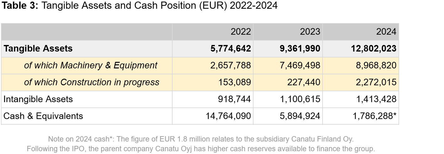
The result is significant growth in tangible assets on the company’s balance sheet. The value of machinery, buildings, and construction in progress grew to €12.8 million by the end of 2024. This represents real, physical infrastructure that cannot be simply replicated overnight and which forms the foundation for future scaling of production and revenue.
The financial picture of Canatu in 2024 portrays a company that is no longer merely a research startup, yet not quite a stably profitable manufacturing firm. It is in a phase of intense transition, characterized by rapidly growing revenue, a clearly defined key market in the semiconductor industry, and significant investments in manufacturing capacity. In this context, operating at a loss does not appear to be a structural problem, but rather a natural consequence of aggressively building the technological and manufacturing foundation for future growth.
Future Revenue
Within the scope of financial analysis and investment reasoning, it is natural to ask what projected revenues Canatu might generate in the future. Regardless of management’s official outlook, making such an estimate is relatively difficult at this stage due to the lack of granular public data.
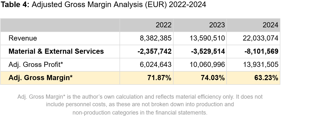
However, looking at the company’s reported figures, we can try to calculate the Gross Margin (specifically Material Margin) to gauge production efficiency. By subtracting material and service costs (€8.1 million) from total revenues of €22.0 million, we arrive at a material margin of approximately 63%. While this is a decrease from the roughly 74% seen in 2023, the drop is logical, the firm began selling hardware (reactors), which is inherently more material-intensive than selling membranes alone. Even so, 63% remains a very healthy figure, indicating a high value-add product.
For this reason, we cannot yet quantify future revenue, margins, or potential profitability with sufficient certainty. This information deficit is largely due to the fact that reactor production is currently in the low-volume, “first-of-a-kind” delivery phase. These units are burdened with one-off development, engineering, and validation costs, expenses that do not persist in long-term unit production. Therefore, margins achieved on the first reactors are of limited predictive value for the company’s future economics.
Nevertheless, we can work with general and defensible estimates based on semiconductor industry practices, and the pellicle demand modeling we did earlier.
The reactors themselves, as physical manufacturing equipment priced in the single to low double-digit millions of euros, can be expected to have lower margins initially, perhaps low or even zero. However, once industrialization and standardization are achieved, these could stabilize at 30% or more, which corresponds to the specialized semiconductor equipment segment.
Significantly more attractive economics likely lie in the consumable materials necessary for pellicle production, where Canatu secures exclusive supply rights for its reactors and where we can realistically expect margins exceeding 60%.
Finally, from an investment perspective, the most interesting component of the business model is the recurring revenue from licensing fees for every pellicle produced. In this case, future revenue will depend on production volume and adoption rates, but this is where we can expect the highest margins, potentially at the level of 80–90% or more.
Is It Expensive? Contextualizing Valuation
At first glance, with a Price-to-Sales (P/S) multiple of around 15x, the stock might seem optically expensive. However, it is crucial to understand that the market is not pricing in current revenue, but rather the monopoly potential at a critical choke point of the global supply chain. For deep-tech companies at the inflection point of adoption, standard metrics often fail to capture the real value. Furthermore, the strategic value of this IP for industry giants like ASML, Applied Materials, or Entegris vastly exceeds the current market capitalization. This strategic scarcity provides investors with a unique safety cushion, an implicit floor on the stock price driven by M&A potential rather than just current cash flow.

SPAC IPO: Dilution Dynamics and Key Price Levels
For investors in Canatu, it is critical to look beyond the current market capitalization and understand the company on a fully diluted basis.
As history has shown, SPACs are often a red flag for many investors. They tend to come with meaningful downsides, particularly when it comes to dilution over time. That concern is valid. At the same time, SPAC transactions also bring substantial upfront capital, which can be crucial for companies operating at the cutting edge of deep technology. In Canatu’s case, this capital helped finance an expensive and technically demanding early phase that would have been difficult to support through organic cash flow alone.
The SPAC listing via Lifeline SPAC I introduced a capital structure with several forms of contingent equity, which can materially increase the share count as the stock price rises. While the commonly cited figure of issued shares reflects the current situation, approximately 34 million shares outstanding, there are mechanisms beneath the surface that are automatically triggered at specific price levels, leading to the issuance of millions of additional shares. Below is a breakdown of the three key components of this structure.
1. Warrants: Capital inflow with dilution
The first layer consists of warrants distributed among founders, sponsors, and investors. Their mechanics are straightforward: the right to subscribe to new shares at a fixed exercise price, in this case set between 11.50€ and 12.00€.
Investor warrants apply to both retail and institutional holders who owned shares in September 2024. A notable feature of the sponsor warrants is the option for net subscription, meaning sponsors do not necessarily inject cash but instead receive the net difference between the market price and the exercise price in shares.
2. Option programs and earn-outs
The most significant, and often overlooked element is the Seller Earn-out. This is a contractual obligation to issue additional shares to Canatu’s original owners at no cost if the company performs well. This pool, together with management option programs, vests in three tranches tied to share price thresholds at 14€, 18€, 22€.
Unlike warrants, earn-outs do not bring any capital into the company. They represent a direct transfer of value from existing shareholders to the original owners.
46 Million Shares
When valuing Canatu, it is worth highlighting the detailed work of Atte Riikola, an analyst at the Finnish investment platform Inderes, who has carefully modeled the impact of these instruments.
His analysis shows the hard math behind the structure: at a share price of around 10€, the share count stands at roughly 34 million. Once the price exceeds 14€, the number of shares jumps by about 30%, to more than 44 million.
Riikola therefore offers a clear recommendation to investors:
“If you invest in Canatu and expect the company to succeed, it makes sense to base your calculations on a share count in the range of 44–46 million.”
At the same time, he points out an important nuance that many investors overlook:
“Warrants can bring capital into the company if exercised through a conventional subscription. Alternatively, when net exercise is used, little cash flows into the company, but dilution is correspondingly lower.”
For investors, the takeaway is straightforward. If you believe in Canatu’s growth, you must accept that the pie will be divided into more slices over time. Target prices and valuations should therefore be modeled on a fully diluted share count of roughly 46 million, rather than the headline number currently displayed by your broker.
It is, in many ways, the price we pay for a well-managed execution of the company’s strategy. Capital is especially important for smaller companies, and when deployed effectively, it can lead to very positive outcomes. It’s also worth keeping in mind that Canatu is a company with a market capitalization of roughly 300 million, where such financing structures are fairly common when growth and expansion are required at this stage. In the end, it comes down to each investor to run the numbers and decide whether this is a price worth paying.
This is how I think about it:
In Canatu’s case, where the business operates in a capital-intensive manufacturing and deep-technology environment that requires substantial upfront investment, I think the structure can make sense. In many ways, it represents compensation for early investors who took on significantly more risk than we are taking today.
My Investment
After weighing all these factors, I decided to invest in the company myself. It strikes me as a secure infrastructure play, a necessity for the future. While retail mania focuses on hyperscalers, which, given their valuations, do not interest me personally at all, I try to look for smaller pieces of the puzzle that AI simply cannot do without.
If Canatu executes its goals, it is safe to say that every chip made on ASML machines for these hyperscalers, using CNT pellicles in EUV production, will contain a tiny sliver of margin for Canatu.
From my perspective, this is a way to carve out a slice of this massive mania for my own portfolio.
Barrier to Entry: Not for Everyone
The fact that this is an overlooked opportunity was confirmed by the very first practical hurdle: I couldn’t buy it.
Although listed on the Nasdaq First North Finland, the shares were not available through commonly used investment platforms. Even on the European version of Interactive Brokers, which usually offers a very broad spectrum of tickers, Canatu shares could not be traded as standard.
Paradoxically, this can be interpreted as a positive signal. Limited availability often means the stock is not yet part of the broader investment mainstream; it lacks retail capital and large US institutional funds, sitting outside the market’s main spotlight. In other words, it is a less beaten investment path.
Eventually, I found that one of the few brokers accessible to the average investor that lists this company is eToro. That is where I finally executed my purchase and started building my position. Kudos to them.
Summary
Investing in Canatu is not a wager on a single isolated product nor a short-term trend. It is exposure to a technology platform that systematically removes key bottlenecks in several of today’s most important structural trends.
Growing demand for more powerful AI and computing power requires the next generations of semiconductor technologies. These are directly dependent on the development of High-NA EUV lithography, whose roadmap is dictated by ASML. Precisely in this critical link of the supply chain, Canatu’s technology becomes an indispensable enabler.
Similarly, in electromobility and autonomous driving, the main limit is not software, but the physical reliability of sensors and energy efficiency. The cleanliness of optical systems, instant functionality under all conditions, and the minimization of energy losses are problems that cannot be solved by an algorithm. Here, Canatu offers a material solution that meets both the regulatory and technical requirements of future vehicles.
It must be openly acknowledged that Canatu remains a small-cap company traded on Nasdaq First North Finland, which entails higher volatility, lower liquidity, and sensitivity to execution risk. However, this very fact is also the source of the asymmetry. If the indications of a dominant position in EUV pellicles, spoken of by management, are confirmed, and if the technology’s application ecosystem continues to expand, the upside potential remains significantly open.
From an investment perspective, Canatu fits into the pick and shovel category, a company that doesn’t bet on the winners of individual races but supplies critical infrastructure to all participants. In an environment where technological races are run in nanometers, joules, and yield, this type of firm can hold disproportionately high strategic importance.
Further concrete information on financial projections, capital allocation priorities, and long-term strategy should be presented at the upcoming Capital Markets Day planned for March. For investors, this could be an important milestone indicating whether Canatu’s technology story will begin to fully translate into financial reality.
A Personal Note
Finally, if you have read this far, I want to thank you sincerely. For me, this journey has reinforced a valuable lesson.
It is crucial to approach investments with a clear philosophical and analytical framework.
Running the numbers and analyzing data is a necessary process, but sometimes the best move is to close the spreadsheets, sit in silence, and simply reflect on how the world is shifting. I started out looking for substitutes for expensive precious metals in mass production. Costly raw materials always squeeze margins, and with silver hitting decade highs, it became a structural problem that inevitably demanded a solution sooner or later.
I never expected my research to lead me to a golden opportunity in semiconductors, a field I am personally passionate about. But that is precisely the joy and education of investing. You learn to understand the world around you.
Let’s see how it all plays out and what changes the world brings tomorrow.
20.1.2026 ~ The Value Philosopher
If you enjoyed this article and want to read more about the intersection of macroeconomics, technology, and investing, consider subscribing.
PART 2: CNT Pellicles Explained: Hydrogen, Lifetime, and the Demand Math
Yesterday I added the Visual Analysis with some new graphs. Today I updated the DRAM section of the model as some industry estimates suggest that, in such a volume-driven wear regime, DRAM-related pellicle demand could approach ~30–40% of the total EUV pellicle addressable market by 2030. Thanks for reading! I hope it's useful.
Tomorrow, I will add some additional visual graphs to my pellicle demand model, for better and clearer understanding. The tables and all the data in it might seem a bit overwhelming.